CHAPTER SEVEN
Creating a 3DIC Design: Three Pieces of Silicon and a Plan That Is Never Built
By the end of this chapter you will be able to say what a 3DIC design is and how a 2.5D design differs from it; to set the one application option that has to be right before the first library is opened, and to work out its value from the libraries you were given; to prepare an active die for mounting, and to know why a fully placed design is not needed; to create a silicon interposer from an empty netlist, populate it with package-facing bumps and give each one a through-silicon via; to assemble a top-level design that places every die at a coordinate and a z level, and to explain why that design is never manufactured; to copy microbumps from a die onto the interposer rather than designing them twice, and to propagate the connections and matching types that make the copies mean something; to read and write the whole bump and via floorplan as a comma-separated file, including the pseudo-bump form used for early planning and the three-file flow used for changes; to build a power mesh under each die; to work out whether the channel between two die is wide enough before anybody agrees the interposer's size; and to run the one check that, unlike every other check in this book, does everything by default.
Why this chapter matters in a real project
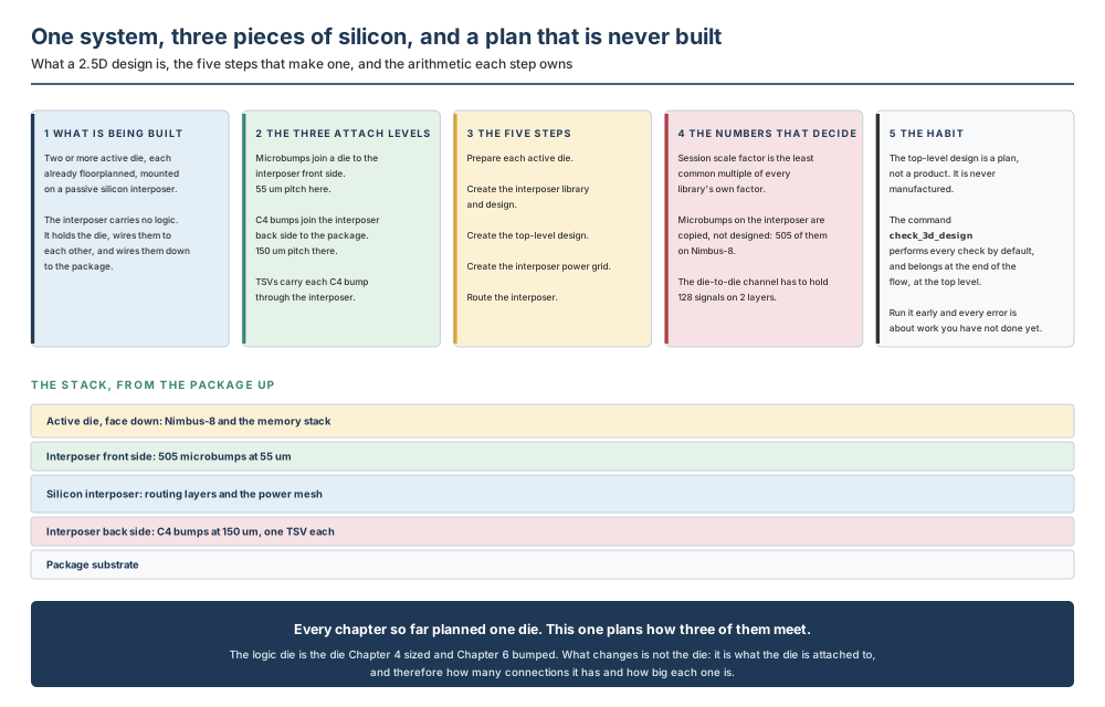
Six chapters have planned one die. This chapter plans how three of them meet.
The reason that matters is not novelty. It is that a system built from several die has several owners, and the interfaces between them are agreed long before anybody can check them. The memory die comes from one team or one vendor; the logic die is yours; the interposer is a third design that exists only to join them; and the package sits underneath all of it with a bump map that was probably signed off first. Every one of those handovers is a number in a document, and this chapter is about turning those numbers into a floorplan that closes.
What makes it worth reading slowly is the same thing that made Chapter 6 worth reading slowly, one level up. In Chapter 6 the pad width came from a library and the bump pitch came from a package, and the arithmetic ran into both. Here the die sizes come from other designs, the microbump pitch comes from the attach process, the C4 pitch and the interposer outline come from the package, and the arithmetic runs into all four. There is a great deal of tooling in this chapter — a dozen commands whose names begin with the same three characters — but almost none of it makes a decision. It records decisions you have already made, and it does so faithfully, including when they were wrong.
The other reason for care is a specific reversal. Chapter 6 ended on a command that checks nothing unless you tell it what to check. This chapter ends on a command that checks everything unless you tell it not to — and which, run at the wrong moment, buries you in errors about work you have not done yet. Two check commands, two opposite defaults, one chapter apart. That is not a trap the tool set out to lay; it is what happens when two commands are written years apart for different jobs. But it is exactly the kind of thing that costs an afternoon, and it is worth knowing before it costs you one.
Prerequisites
Chapter 4, for the die and core boundary and how initialize_floorplan creates one. Chapter 6, for bump cells, bump arrays, matching types and redistribution-layer routing — this chapter reuses all of them and assumes you can read a create_bump_array command without looking it up. Chapter 8 covers design blocks and the library structure in earnest; here you need only to know that a design lives in a library, that a library can reference other libraries, and that a block has to be editable before you can change it.
Nothing in Chapters 3 or 5 is needed. If you have read them, one thread does carry over: a black box was a module whose contents were unknown but whose interface was fixed, and an active die that somebody else owns is the same idea with a boundary instead of a netlist.
How to read the numbers and the notation in this chapter
This is the same table that opens every chapter, with the entries this chapter actually needs. Nothing in it is difficult; it is here so that no symbol on the page is ever a puzzle.
| You will see | Read it as | What you need to know |
|---|---|---|
| µm | microns, or micrometres | A length, one thousandth of a millimetre. Every command in this chapter is typed in these. The interposer in the worked example is 10,000 µm wide, which is 10 mm — a full centimetre of silicon. |
| mm | millimetres | Used only when a figure needs to feel like a real object, and always with the micron value beside it. 1 mm = 1,000 µm. |
| mm² and µm² | square millimetres and square microns | Areas. Every area in this chapter is printed twice, once in each, because a human estimates in mm² and a tool is typed in µm². 1 mm² = 1,000,000 µm². |
| × ÷ − + | multiply, divide, subtract, add | Ordinary arithmetic with the proper signs, so a multiplication is never mistaken for the letter x and a subtraction is never mistaken for a hyphen in a command option. |
| 10,000 | ten thousand | Commas group digits in threes so a long number reads at a glance. They are punctuation only: typed into a command the same number is bare, 10000, and a comma there is an error. |
| a square 3,440 µm on each side | a square whose sides are each 3,440 µm long | A shape and a length, not an area. Its area is a separate number and this chapter always states it separately. |
| z 0, z 1 | z level zero, z level one | The stacking order, not a height in microns. Level 0 is the piece nearest the package. Two things at the same level sit side by side; two things at adjacent levels sit one on top of the other. |
| Section 7.4.3 | section 7.4.3 of this chapter | A cross-reference. The first digit is the chapter, so anything beginning “7.” is in these pages. |
| derive_3d_interface | a command, exactly as typed | Anything in this typewriter face is something you type, or a name the tool uses. Reproduced character for character: spelling and underscores matter. |
| -z_offset | an option belonging to a command | The leading hyphen marks it as an option, not a subtraction. Options follow the command name, in any order, each with its value after it where it takes one. |
| {{0 0} {10000 6000}} | a nested Tcl list holding two points | Curly braces group things. The outer braces hold the whole list; each inner pair holds one coordinate pair, here the lower-left and upper-right corners of a rectangle. |
| C4 | see four | The name of a bump type, not a formula. It stands for Controlled Collapse Chip Connect, and in this book it always means the large, package-facing kind of bump. |
Learning objectives
- Define a 3DIC design and a 2.5D design, and say which one this chapter's flow builds.
- Name the seven terms in the chapter's own glossary — interposer, active die, front side, back side, through-silicon via, microbump, C4 bump — and point at each one on a cross-section.
- Compute a session scale factor from a set of library scale factors, and say what happens if you get it wrong.
- List the five steps of the 2.5D flow in order and name the command that performs each one.
- Create an interposer design from an empty netlist and explain why the netlist may be empty.
- Place three instances at coordinates and z levels with
set_cell_location, read the result back withreport_3d_chip_placement, and say which pairs of that command's options are mutually exclusive. - Copy microbumps onto an interposer with
create_3d_mirror_bumpsand name the four commands that turn those copies into connected, matched nets. - Read and write a bump and via floorplan as a comma-separated file, and state the default overlap rules the reader applies.
- Build a power mesh under each die with a pattern, a strategy per die and one
compile_pg, and count the straps it will produce. - Work out whether a die-to-die channel is wide enough, from a signal count, a layer count and a track pitch, before the interposer size is agreed.
- Run the ten checks of
check_3d_design, and explain why its default is the opposite ofcheck_io_placement's.
7.1 The beginner's mental model
Start with a power strip
Put a kettle and a radio on a desk, and plug both into a power strip whose lead runs to a socket in the wall.
The kettle and the radio do the work. The strip does none: it carries current, and that is all it is for. It has a face covered in sockets, one set for each appliance, and a single thick lead with one big plug on the end of it going off to the wall. Nobody designed the socket holes from scratch — they are a mirror image of the pins on the plugs that go into them, and if the pin pattern changes the hole pattern has to change with it.
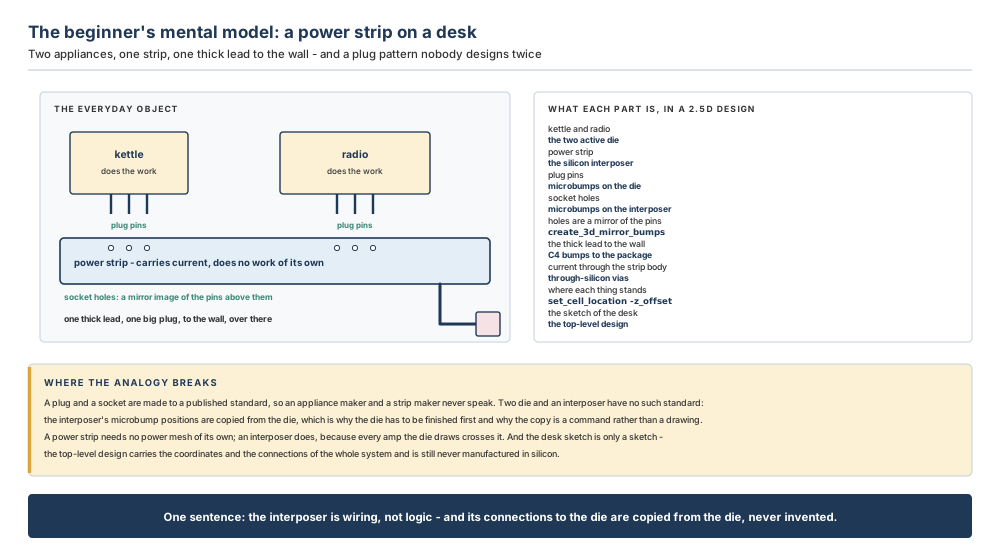
A plug and a socket are made to a published standard. That is why an appliance factory and a power-strip factory never need to speak to each other. Two active die and an interposer have no such standard: the interposer's microbump positions are copied from the die, which is why the die has to be substantially finished before the interposer can be populated, and why the copying is done by a command rather than by a draughtsman.
A power strip also needs no power distribution of its own — the wire in it is the wire. An interposer does, because every amp both die draw has to cross it, and Section 7.4.6 builds a mesh for exactly that reason.
And the desk sketch is only a sketch. The top-level design is more than that: it holds the coordinates, the orientations, the z levels and every connection in the system. It is still never manufactured.
Now the engineering model
A 3DIC design is one in which two or more die are directly stacked vertically to create a complete design or system containing multiple die. A 2.5D design is one in which one or more die are mounted on an interposer, and the interposer connects the die to each other and to the package. The interposer can be manufactured from various materials, including silicon and glass.
Both styles are supported, and the die can be placed separately on a silicon interposer or stacked upon each other and connected with through-silicon vias. The flow this chapter follows is the 2.5D one — active die placed side by side on a passive silicon interposer — because it is the one the framework works through end to end, and because everything it teaches transfers to the stacked case.
Two pieces of vocabulary come from that definition and are worth fixing now. An active die is a die containing active devices: logic, memory, radio-frequency circuitry, anything with transistors in it. The interposer is the silicon die that mounts and connects the active die, and it is not required to contain active components or logic at all. In the flow below it contains none: its netlist is literally empty when you create it.
The word “passive” does a lot of work in that last paragraph, and it is worth being precise about what it does and does not mean. A passive interposer has no transistors. It does have metal — several routing layers of it — and it has bumps on both faces and vias through its body. It is a printed circuit board's job done in silicon at silicon's dimensions, and everything in this chapter that feels like board design rather than chip design is that resemblance showing through.
Do not confuse these
Ten pairs that get mixed up, and the one-line difference in each case. This table is worth a second read after Section 7.5, when the pairs have names attached to them.
| These two | Are not the same thing |
|---|---|
| 3DIC and 2.5D | In a 3DIC design two or more die are stacked vertically. In a 2.5D design one or more die are mounted on an interposer, which connects them to each other and to the package. The tool supports both, and this chapter's flow is the 2.5D one. |
| Microbump and C4 bump | Both are single-pin cells on a front or back side. A microbump carries the redistribution-layer metal and joins a die to the interposer. A C4 bump carries the back-side metal and joins something to the package. In the worked example one is at 55 µm pitch and the other at 150 µm, so their counts differ by a factor of three. |
| Front side and back side | The front side is the top side of a die, opposite the substrate and device layers, where most of the standard-cell metal routing is performed. The back side is the bottom side, containing the substrate and device layers, where the back metal layers are created. On an interposer, microbumps sit on the front and C4 bumps on the back. |
| A through-silicon via and an ordinary via | An ordinary via joins two metal layers. A through-silicon via connects the back-side metal through the substrate with the device layers to the front-side metal — it crosses the whole die. TSVs are required on the interposer to propagate signals from the package substrate through to the die. |
| The interposer design and the top-level design | The interposer is a real design that is manufactured. The top-level design instantiates the interposer and every active die, holds the coordinates and connections, and is never manufactured in silicon. Its design_type is 3dic; the interposer's is not. |
-z_offset and a height in microns | -z_offset specifies the stack order of a physical cell, not a distance. Two cells at the same z value are at the same elevation and are checked for overlap; two at adjacent z values are neighbours and are checked for physical contact. |
| A library scale factor and the session scale factor | Each library has its own scale factor. design.session_scale_factor is the one value the whole session uses, and it must be a multiple of every library's. Set it before the first design library is opened or created, or a library with a different factor causes an error and an exit. |
| A bump and a pseudo bump | A bump is a cell instance. A pseudo bump is a planning object living inside a bump region, with a shape and a radius rather than a library cell, used to lay out a bump field before the cells exist. Both can be written to and read from a comma-separated file. |
propagate_3d_connections and assign_3d_interchip_nets | The first creates logical connections between the new interposer bumps and the bumps on the active die. The second assigns bumps to their nearest drivers, creates the ports and nets in the interposer from the top-level connectivity, and creates the feedthroughs. One wires up what you copied; the other decides what connects to what. |
check_io_placement and check_3d_design | Chapter 6's check performs only the checks you name. This chapter's performs all of them unless you exclude some, and belongs at the last step of the flow, run at the top level. Two commands, two opposite defaults. |
7.2 The concepts, from first principles
7.2.1 The seven words, and where each one is
This chapter has more new vocabulary than any other in the book, and almost all of it is spatial. That makes it easy — you can point at every term on a single cross-section — and it makes it dangerous, because a term you can only half place is worse than one you cannot place at all.
So here are all seven, on one drawing, with the reference's own definition of each beside it.
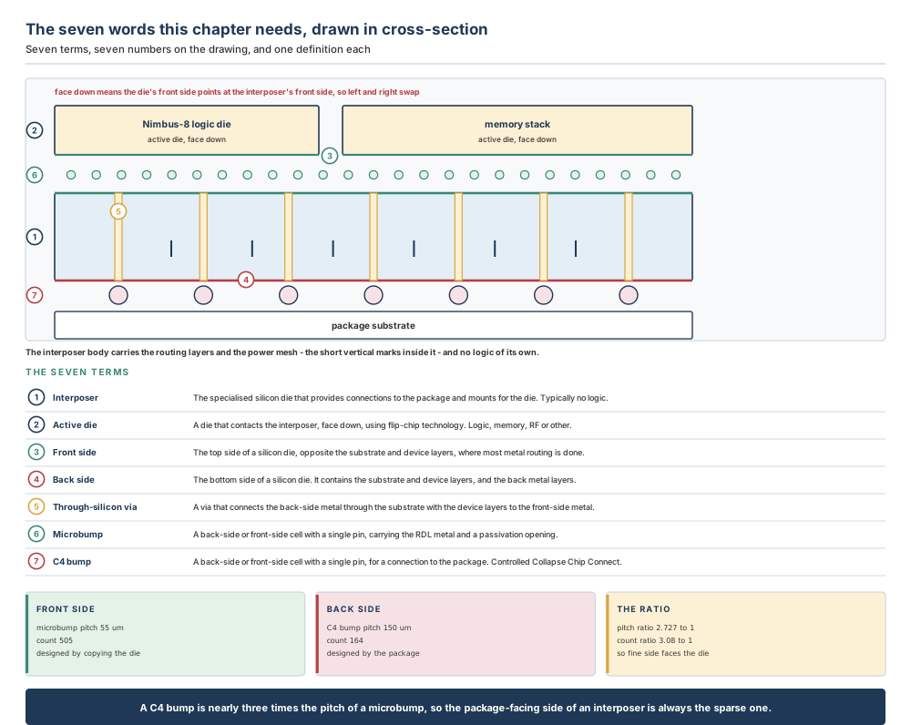
Two of the seven repay a second look.
Front side and back side are not top and bottom of the assembly. They are properties of a die. The front side is the top side of a silicon die, opposite the substrate and device layers, where most of the standard-cell metal routing is performed. The back side is the bottom side, containing the substrate and device layers, where the back metal layers are created. So “front” means the metal-stack face and “back” means the substrate face, whichever way up the die happens to be sitting. An interposer's front side faces up towards the die; an active die, mounted face down, has its front side facing down towards the interposer. The two front sides meet.
Because the active die is mounted face down, its coordinate system is flipped relative to the interposer's. Left and right swap. This is the same flip Chapter 6's flip-chip designs had, but it matters more here, because in Chapter 6 you only had to get one die's bumps right and here you have to get two die's bumps to agree with each other through a third design that sits between them. The orientations in the worked example are FN for both active die and N for the interposer, and that is not decoration.
The pitch ratio is the whole shape of the problem. A microbump joins a die to the interposer; a C4 bump joins the interposer to the package. In the worked example the microbump pitch is 55 µm and the C4 pitch is 150 µm — a ratio of about 2.727 to 1 — so a given area of interposer holds roughly seven times as many microbumps as C4 bumps. That is why 505 microbumps sit on the front side and only 164 C4 bumps on the back, and why the back side of an interposer always looks empty next to the front. It is also why the interposer exists: something has to fan out from a coarse package pitch to a fine die pitch, and that something is metal on silicon.
7.2.2 The flow, and the commands each step owns
The flow for a 2.5D design with active die placed separately on a passive silicon interposer has five steps: prepare the designs for the active die; create the interposer library and design; create the top-level design; create the interposer power grid; and route the interposer.
Five steps is an unusually honest number for a flow diagram, because each of the five is a genuinely separate piece of work with its own inputs and its own owner. The first step is done once per die and can be done in parallel. The second creates a design that does not exist yet. The third is the only one that sees the whole system. The fourth and fifth are ordinary physical design done on an unusual object.
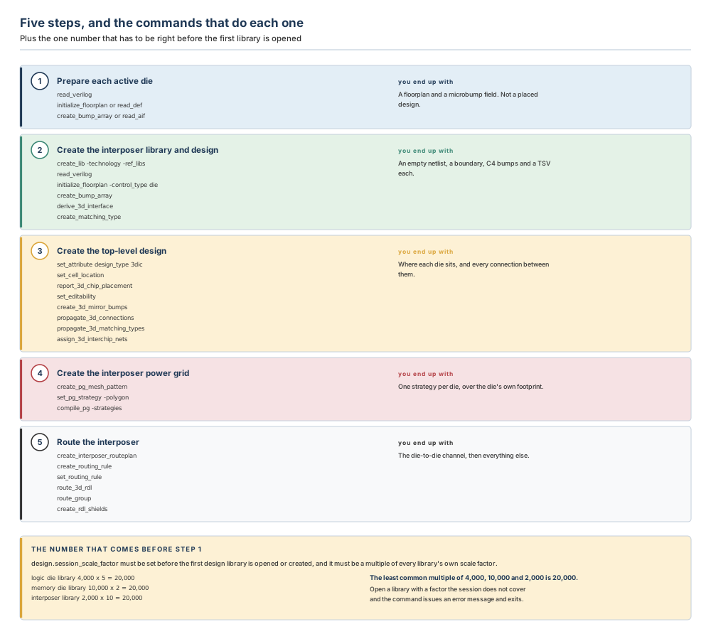
Table 7.3 is the same information as a list you can scan while writing a script, with the section that treats each command in full.
| Command | Step | What it does |
|---|---|---|
| create_lib | 2, 3 | Creates the design library for the interposer, and later for the top level, naming the technology file and the reference libraries it depends on. |
| derive_3d_interface | 2 | Creates new 3DIC structures from the properties of existing ones. Used here to give every C4 bump a through-silicon via. |
| read_design_io | 2, 3 | Reads bump, microbump and TSV placement and connection information from one or more comma-separated files and places the cells. |
| write_design_io | 2, 3 | Writes that same information out. With -pseudo_bumps, writes the bump-planning form instead. |
| compare_design_io | 3 | Compares two versions of a bump floorplan given as two files, and writes the differences out as a third. |
| set_cell_location | 3 | Places a die instance at a coordinate, an orientation and a z level in the top-level design. |
| report_3d_chip_placement | 3 | Reports the placement information set_cell_location set, one row per die. |
| set_editability | 3 | Makes the referenced blocks editable, which they must be before the top level can add bumps to them. |
| create_3d_mirror_bumps | 3 | Copies and places bump cells, bump clusters and bond pads from a source die to a target die. |
| propagate_3d_connections | 3 | Creates the logical connections between the copied bumps and the bumps they were copied from. |
| propagate_3d_matching_types | 3 | Copies matching types of cells, pins and terminals to other pins, from one die to the others. |
| assign_3d_interchip_nets | 3 | Assigns bumps and pseudo bumps to their nearest drivers, creates the interposer's ports and nets from the top-level connectivity, and creates feedthroughs. |
| create_3d_virtual_blocks | 3 | Creates the virtual interface block that holds the cross-coupling capacitance between two stacked die. |
| check_3d_design | 3 | The chapter's check. Ten categories, all of them on by default, run at the top level at the end of the flow. |
| create_pg_mesh_pattern | 4 | Defines a mesh pattern: which layer runs which way, and the width, spacing, pitch and offset of the straps. |
| set_pg_strategy | 4 | Associates a pattern with a region — here, the footprint of one die — and with a pair of nets. |
| compile_pg | 4 | Instantiates the power plan the strategies describe. |
| create_interposer_routeplan | 5 | Analyses the placed and assigned bumps and creates the vias, and optionally the route guides, that the router will follow. |
| route_3d_rdl | 5 | Routes the redistribution-layer nets on a named layer, optionally inside a named region only. |
| route_group | 5 | Routes the interposer's lower metal layers with Zroute, after set_ignored_layers has narrowed the layer range. |
| create_pseudo_bump | 2 | Creates one planning bump inside a bump region, with a shape and a radius rather than a library cell. |
| define_user_attribute | 2 | Defines an extra column for the comma-separated file, so a planning attribute of your own survives a write and a read. |
Two commands in that table were already familiar and are doing new jobs. create_bump_array from Chapter 6 populates both the die and the interposer here, unchanged. create_matching_type, also from Chapter 6, is used twice in this chapter — once on the interposer and once at the top level — and then copied between die by propagate_3d_matching_types. If Chapter 6's matching types felt like an optional refinement, this is where they become structural: a 3DIC design's connections are described by matching types, and one of the ten checks is about nothing else.
7.2.3 Libraries, scale factors, and the number to get right first
A 3DIC design contains multiple subdesigns, and each subdesign can reference unique libraries and use a different technology. Those libraries might have different scale factors, and they still have to be used together in the complete design.
A library's scale factor is the number of database units it uses per micron. A library with a factor of 4,000 stores coordinates in units of a quarter of a nanometre; one with 10,000 stores them in units of a tenth of a nanometre. Neither is wrong, and a design assembled from both has to pick a single resolution fine enough to represent every coordinate in either exactly.
That resolution is design.session_scale_factor, and there are two rules about it. It must be specified before the first design library is opened or created. And the scale factors for the various libraries in a 3DIC design must be a multiple of the scale factors of all the libraries — so the option's value has to be the least common multiple of them all, or an even multiple of that.
# Set this first. Before create_lib, before open_lib, before anything.
icc2_shell> set_app_options -name design.session_scale_factor \
   -value 20000
Where does 20,000 come from? Not from anywhere; you work it out. The Nimbus-8 system has three libraries:
# From the three library owners.
logic die library        scale factor  4,000
memory die library       scale factor 10,000
interposer library       scale factor  2,000

# The smallest number all three divide into exactly. Start at the
# largest factor and step through its multiples.
10,000  ->  10,000 / 4,000 = 2.5      no
20,000  ->  20,000 / 4,000 = 5        yes
            20,000 / 10,000 = 2       yes
            20,000 / 2,000 = 10       yes

# So the session scale factor is 20,000, and an even multiple of it
# would also be legal: 40,000, 60,000 and so on.
The framework gives the same shape of example with two libraries: if one library has a factor of 4,000 and another has 10,000, the option must be set to the least common multiple, 20,000, or an even multiple of it. Adding a third library at 2,000 does not change the answer here, because 20,000 was already a multiple of 2,000 — which is worth noticing, because it means adding a library sometimes costs nothing and sometimes changes the whole session.
By default this option is not set, and if you open a library with a different scale factor the command issues an error message and exits. Not a warning, not a skipped step: the session ends. This is the only command in seven chapters that behaves that way, and it is the reason the option belongs in the first ten lines of the setup script rather than anywhere near the flow.
The remedy is not to guess a large round number. A session factor that is a multiple of every library's factor but much larger than necessary wastes coordinate range for no benefit. Ask each library's owner for its factor, take the least common multiple, and write the arithmetic in a comment beside the option so that the next person to add a library knows what to recompute.
There is a second scaling mechanism for half-node libraries. The half-node scale factor of a library is specified by the half_node_scale_factor attribute on the library. If design.is_3dic_mode is set to true on the top design, the coordinates in the library are scaled by the half_node_scale_factor setting when the library is read. That is the whole mechanism: an attribute on the library, an application option to enable it, and the scaling happens at read time.
Why would a library need scaling at all, rather than simply being drawn at the right size? Because a half-node process is a shrink of a full node, and the library for it is often derived from the full-node library rather than redrawn. Scaling at read time means one library serves both, and the design that consumes it does not have to know which it got. It also means that if the option is off, the same library reads at the wrong size — silently, because nothing about a coordinate says what it was supposed to be.
7.2.4 Preparing an active die
Each active die has an initial floorplan and contains the bump cells used to connect it to the interposer or to another active die. Preparing one is a short flow, and it is deliberately shorter than you would expect:
# 1. The netlist.
icc2_shell> read_verilog logic.v

# 2. A floorplan, created or read.
icc2_shell> read_def logic.def

# 3. The bump cells.
icc2_shell> create_bump_array -lib_cell UBUMP -name ubump_hbm \
   -delta {55 55} -bbox {{2900 640} {3285 1520}}
The framework is explicit about why that is enough: it is not necessary to create a fully placed design, since the critical pieces of information for placing the active die on the interposer are the bump cell locations and the active die size. Those two things are the interface. Everything else about the die — where its blocks sit, how its clock is built, whether it meets timing — is the die owner's business and invisible from the interposer.
Bump cell locations can come from three places, exactly as in a flip-chip design: a DEF file, an AIF file, or the create_bump_array command. And the redistribution-layer routes from pad cell to bump cell can be created during a later design stage — so a die can be handed over with its bumps placed and nothing routed to them yet.
What changes if the die was already bumped for direct flip-chip attach, as Nimbus-8 was in Chapter 6?
Then its bump field has to be redone, and this is the most consequential decision in the chapter. Chapter 6 gave Nimbus-8 305 bumps at a 150 µm pitch, sized for a package. An interposer attaches at a much finer pitch — 55 µm in this chapter — so the same 305 connections now occupy roughly a seventh of the area they did, and they no longer need to reach the die's periphery at all.
What does not change is the count. 192 signal connections are 192 signal connections whatever they are attached to, because that number came from the netlist. 113 power and ground connections came from the current the die draws. So Nimbus-8 arrives in this chapter with the same 305 bumps it left Chapter 6 with, rearranged into a much smaller field. Section 7.5 does that rearrangement, and the fact that the total is unchanged is the check that it was done honestly.
7.2.5 The silicon interposer design
Creating the interposer means creating its library, creating its netlist, initialising its floorplan and creating its power and ground connections. Six commands, and the second one is the surprising one.
# 1. The library, naming every reference library the interposer needs.
icc2_shell> create_lib nimbus_interposer.ndm \
   -technology interposer.tf \
   -ref_libs {c4_bump.nlib front_ubump.nlib physicalonly.nlib}

# 2. An empty netlist. Yes, empty.
icc2_shell> sh cat interposer.v
module interposer (dummypin);
input dummypin;
endmodule
icc2_shell> read_verilog interposer.v

# 3. The boundary, in the tool's unit.
icc2_shell> initialize_floorplan -control_type die \
   -boundary {{0 0} {10000 6000}}
An interposer's netlist is empty because the interposer has nothing in it to describe. Its content is bumps, vias and metal, all of which are physical objects created by later commands, and its connectivity comes from above: the top-level netlist contains the connections, and the tool automatically updates the interposer netlist with ports and all connections and creates feedthroughs as needed.
That is a genuinely unusual arrangement and worth sitting with for a moment. Every other design in this book was created from a netlist that described it. This one is created from a stub, and is filled in by a command that runs in a different design. If you have ever wondered what “physical only” really means, this is the extreme case of it.
Then the package-facing bumps and their vias:
# 4. C4 bumps, to the package. The pitch came from the package.
icc2_shell> create_bump_array -lib_cell C4_BUMP \
   -name c4_sig_bottom -origin {125 75} -delta {150 150} \
   -repeat {8 8}

# 5. One TSV for each of the bump cells just added.
icc2_shell> derive_3d_interface -from [get_cells c4_sig_bottom*] \
   -to_object_ref [get_via_defs -tech [get_techs *] VIA_TSV] \
   -name_prefix TSV_c4_sig_bottom

# 6. Matching types, for the RDL routing that comes later.
icc2_shell> create_matching_type \
   -name Signal [all_connected [get_nets *SIG*]]
derive_3d_interface is the command that repays study, because its name is doing something unusual. It creates new 3DIC structures based on the properties of existing structures in the design. You do not tell it where to put the vias; you tell it which existing objects to derive from with -from, and what to make with -to_object_ref, and it places one new object per source object, inheriting position from the source. Options let you shift the result with -x_offset and -y_offset, choose which corner or centre the offsets are measured from with -coord_spec, decide whether the new object is connected with -connect, name the results with -name_prefix, set an orientation, and give a bond pad a width and height.
“One per source object” is why the TSV count in this chapter is not an independent number. There are 164 C4 bumps on the Nimbus-8 interposer, so derive_3d_interface creates 164 TSVs. If somebody adds four more C4 bumps for a late power requirement and forgets to re-run the derive step, the design has 168 bumps and 164 vias, four of the bumps connect to nothing, and no message says so until the connectivity check runs at the very end. Re-running the derive is cheap. Finding out at the end is not.
7.2.6 The top-level design
A 3DIC design contains two or more active die and a silicon interposer, and both are instantiated into a top-level design. That design also contains the connections between the package, the interposer and the die, as well as the ports that represent connections to the package.
And then the sentence that defines the whole object: the top-level design specifies only the physical and logical connectivity between the actual die and the interposer; the top-level design is never actually manufactured in silicon.
What you can do with it is a five-item list worth memorising, because it is also a list of everything in this chapter that requires a whole-system view: specify the coordinates and orientation of the die on the interposer; copy or mirror bumps between the interposer and the die; perform 3D physical and logical design checks of the entire system; assign bumps to signals based on the shortest paths; and report information about valid 3D chips.
![On the left, headed side elevation by z level, a drawing: at z 1, a yellow box labelled logic_die_inst captioned Nimbus-8 and a green box labelled mem_die_inst captioned memory stack, side by side; at z 0 below them, a wider pale blue box labelled interposer_inst captioned the only one that touches the package. A caption reads: same z level means the two must not overlap, adjacent z levels mean they are checked for physical contact, the z values must start at 0 and be continuous. On the right, headed what puts them there, a command listing: set_attribute [current_block] design_type 3dic; then set_cell_location interposer_inst -coordinates {0 0} -z_offset 0 -orientation N; set_cell_location logic_die_inst -coordinates {400 1280} -z_offset 1 -orientation FN; set_cell_location mem_die_inst -coordinates {4100 600} -z_offset 1 -orientation FN. Below, headed what report_3d_chip_placement gives back, a six-column table with columns chip_name, design_type, stack_z, location, orientation and scaling_factor, and three rows: logic_die_inst die 1 (400 1280) FN 1; mem_die_inst die 1 (4100 600) FN 1; interposer_inst die 0 (0 0) N 1. Below, three cards. Mutually exclusive pair one, in green: -coordinates gives the lower-left corner of the cell's boundary, -origin gives the cell's origin, you may use one never both. Mutually exclusive pair two, in gold: -z_offset states the stack order outright, -raise -lower -top and -bottom move it by one or to an end, again one or the other. The thing to remember, in pink: the top-level design specifies only the physical and logical connectivity between the die and the interposer, it is never actually manufactured in silicon. A navy band at the foot reads: a top-level 3DIC block is a drawing of an assembly, its design_type is 3dic, and no mask is ever made from it.](/design-planning/assets/ch07_fig06_toplevel.svg)
Building it takes the sequence below. Steps 1 to 4 are ordinary; step 5 is the one this section is about.
# 1. A library that references the interposer and every active die.
icc2_shell> create_lib nimbus_top.ndm -technology top.tf \
   -ref_libs {nimbus_logic.ndm nimbus_mem.ndm nimbus_interposer.ndm}

# 2 and 3. The netlist and a boundary the size of the interposer.
icc2_shell> read_verilog nimbus_top.v
icc2_shell> initialize_floorplan -boundary {{0 0} {10000 6000}}

# 4. Mark this block as a top level or container hierarchy level.
icc2_shell> set_attribute [current_block] design_type 3dic

# 5. Place the interposer and the die, with a z level each.
icc2_shell> set_cell_location interposer_inst \
   -coordinates {0 0} -z_offset 0 -orientation N
icc2_shell> set_cell_location logic_die_inst \
   -coordinates {400 1280} -z_offset 1 -orientation FN
icc2_shell> set_cell_location mem_die_inst \
   -coordinates {4100 600} -z_offset 1 -orientation FN
The z level is the new idea, and it is simpler than it sounds: it is a stack order, not a height. Chips with the same z value are considered to be at the same elevation and are checked for chip overlaps. Chips with adjacent z values are considered to be neighbouring chips and are checked for physical contact. So giving both active die -z_offset 1 declares that they sit side by side and must not overlap, and giving the interposer -z_offset 0 declares that it is underneath both and touches both.
| Option | What it specifies | Worth knowing |
|---|---|---|
| -coordinates | The lower-left coordinates of the boundary of the specified cells, in microns relative to the chip origin | Mutually exclusive with -origin, and cannot be given with -raise, -lower, -top or -bottom |
| -origin | The origin of the specified cells, in microns relative to the chip origin | The other half of that pair. Which one you want depends on where the cell's origin is |
| -center | That the value in -coordinates is the centre of the cells rather than the lower-left corner | Requires -coordinates. Useful when a die's centre is the number you were given |
| -z_offset | The stack order, or z offset, of the physical cell | Cannot be given with -raise, -lower, -top or -bottom |
| -raise | Raises the cells by one position in z level | The relative form. Cannot be combined with -coordinates, -origin or -z_offset |
| -lower | Lowers the cells by one position in z level | Same exclusions |
| -top | Raises the cells to the top of the position stack | Same exclusions |
| -bottom | Lowers the cells to the bottom of the position stack | Same exclusions |
| -orientation | The new orientation | FN for a die mounted face down in this chapter's example; N for the interposer |
| -rotation | A rotation angle | An alternative way to express the same thing for cases the orientation names do not cover |
| -fixed | That the placement is fixed | Worth setting on a die whose position was agreed with the package |
| -ignore_fixed | Sets the location even for cells with fixed placement status | The escape hatch from the line above. Use it deliberately |
| -mirror | Mirrors the cells | Another route to the same flip that FN expresses |
| -design | The design to act in | Rather than the current one |
Reading the placement back is one command, and the report is worth keeping:
icc2_shell> report_3d_chip_placement -chips \
   {logic_die_inst mem_die_inst interposer_inst}
chip_name        design_type  stack_z  location       orientation  scaling_factor
logic_die_inst   die          1        (400 1280)     FN           1
mem_die_inst     die          1        (4100 600)     FN           1
interposer_inst  die          0        (0 0)          N            1
The command reports only block instances at the top level unless you add -hierarchical, which reports all hierarchical die. -application reports each chip's level-layer map information and thickness attributes; where that map has not been set by the user, the command reports the chip's highest front-side metal layer and lowest back-side metal layer instead, in the same format and beginning with an asterisk. The z ordering can also be queried directly as the z_order attribute on a die instance.
Why does a design that is never manufactured need a boundary at all? Because the checks need one. The chip-placement check compares the coordinates of the die against each other and against the top level, and the rule for neighbouring die is that the chip with the larger virtual top-level area should contain the other one. Without a boundary the words “larger” and “contain” have nothing to refer to. The boundary is scaffolding for checking, not a description of a thing.
design_type is 3dic, and it is never manufactured — but it still needs a boundary, because the checks measure against one.7.2.7 Virtual interface blocks
A 3DIC design contains capacitance due to cross-coupling between two die, and that capacitance affects nets at the top level. Extraction tools capture it and store it in a virtual interface block added to the design database — but the block has to exist first, and creating it is a command in this tool.
A virtual interface block contains the ports, nets, shapes and vias at the interfaces between two stacked die, and between a die and the interposer. Three forms of the command cover the cases:
# Between two named blocks, with a layer count for each.
icc2_shell> create_3d_virtual_blocks \
   -blocks {{mem_die_inst:4} {interposer_inst:2}}

# Between two blocks, with the same layer count for both.
icc2_shell> create_3d_virtual_blocks \
   -blocks {logic_die_inst mem_die_inst} -layers 4

# Between every die and the interposer, based on the z offsets,
# and connected into the top-level netlist.
icc2_shell> create_3d_virtual_blocks -in_netlist
The first two add the interface information; -in_netlist modifies the netlist and connects it, creating the blocks between all die and the interposer based on the z-offset attribute setting for each block. There is also a -die_separation option for the separation value between die.
On the Nimbus-8 system that gives two virtual interface blocks — logic die to interposer, and memory die to interposer — because those are the two die pairs at adjacent z levels. The two active die are at the same z level and do not face each other, so no block is created between them.
7.3 Inputs, outputs and readiness
A 3DIC design has more prerequisites than any other step in this book, and most of them belong to other people. This section is the list, in the order things are needed.
| Stage | What has to be true | Who owns it, and what happens if it is wrong |
|---|---|---|
| Before the first library | The scale factor of every library in the system is known, and design.session_scale_factor is set to their least common multiple or a multiple of it. | The library owners. Open a library the session factor does not cover and the command errors and exits. |
If any library is half-node, its half_node_scale_factor attribute is set and design.is_3dic_mode is true on the top design. | The library owner. Otherwise the library reads at the wrong size, silently. | |
| Before the interposer | Every active die has a boundary and a placed microbump field. A fully placed design is not required. | Each die owner. A die without bumps cannot be mirrored from. |
| The microbump pitch is known, and both die use the same one on their facing bands. | The attach process. Two different pitches on a facing pair cannot connect. | |
| The interposer outline and the C4 pitch are known. | The package. Both are usually fixed before the floorplan is. | |
| The die-to-die signal count, the number of routing layers and the track pitch are known, and the channel between the die has been shown to hold them. | You. This is the arithmetic in Section 7.4.6, and nothing later will do it for you. | |
| Before the top level | The interposer library and every die library exist and are named in the top-level library's -ref_libs. | You. A missing reference library makes the instance unresolvable. |
Every referenced block has been made editable with set_editability. | You. The mirror step writes into the target block and cannot if it is locked. | |
The top-level block's design_type is 3dic. | You. It is what marks the block as a top level or container hierarchy level. | |
| Before the power grid | Every die has a placement, so its footprint is a polygon you can name. | You. A strategy with no region has nothing to fill. |
| Before routing | Bumps are placed and assigned, the routing rules exist and are applied to the nets, and the routing angle and design style are set deliberately. | You. An unassigned bump is not an unrouted bump; it is a bump nothing was trying to reach. |
| Afterwards you have | Three manufacturable designs and one that is not: two active die with microbumps, an interposer with microbumps on the front, C4 bumps and TSVs on the back, a power mesh and routes, and a top-level assembly holding it together. | Ten check categories, and the artefacts to prove each one ran. |
A preflight checklist worth running before the first command of the session, in this order. One: collect the three scale factors and compute the least common multiple. Two: confirm the interposer outline and the C4 pitch in writing, from the package owner, with a date on it. Three: confirm the microbump pitch, and that both facing bands use it. Four: count the die-to-die signals, divide by the layer count, multiply by the track pitch, and compare the answer with the gap the outline leaves. Five: count the signal microbumps on each die and check that the two facing counts are equal. Six: confirm every die's bump field is placed and the boundary is final.
Items one and four are the two that end projects. Item one ends the session immediately, which is the kind you find out about. Item four ends it in three weeks, when the interposer outline has been agreed with a package that has already been ordered.
7.4 The guided tool walkthrough
7.4.1 create_3d_mirror_bumps — copying, not designing
Purpose. Copy bump cells from one die onto another die, or onto the interposer, so that the two faces have matching connection points. When the source and target die are stacked vertically, the command copies and places bump cells, bump clusters and bond pads from the source die to the target die.
Syntax in plain English. Name a source chip with -from, a target chip with -to, and the library cell to instantiate on the target with -ref_cell. Both -from and -to are required, and -ref_cell is required when you are mirroring bumps. Add -prefix so the new instances are identifiable.
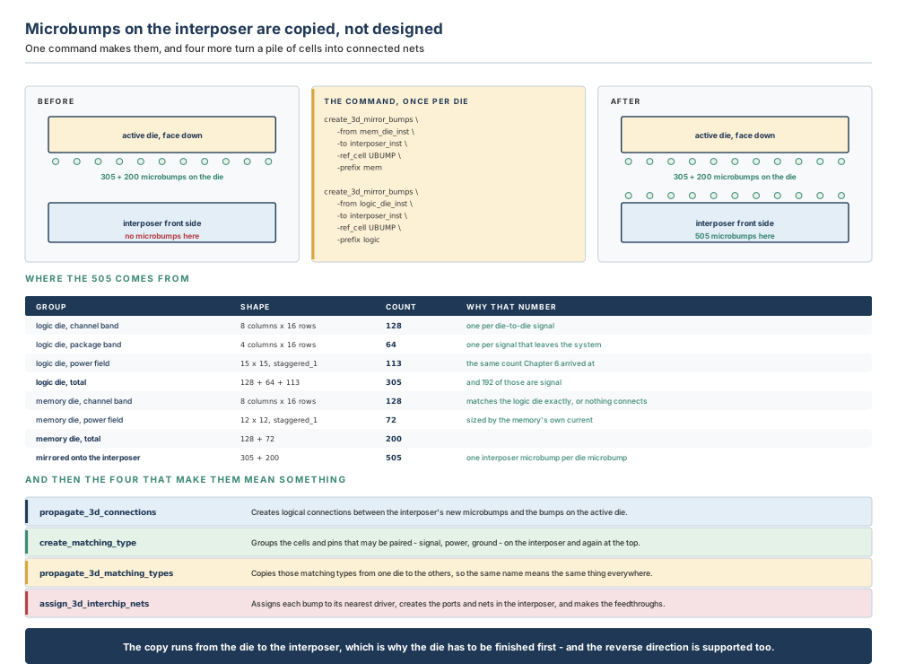
# Once per die. The interposer gains a microbump for every
# microbump on the die that faces it.
icc2_shell> create_3d_mirror_bumps -from mem_die_inst \
   -to interposer_inst -ref_cell UBUMP -prefix mem
icc2_shell> create_3d_mirror_bumps -from logic_die_inst \
   -to interposer_inst -ref_cell UBUMP -prefix logic
The options that matter. Table 7.6 covers the ones that change what gets copied and what it is called. The command has more, and the pattern is worth seeing: almost every option is either “copy this subset instead of everything” or “name the results this way instead of that way”.
| Option | What it does | Worth knowing |
|---|---|---|
| -from | The source chip or sub-block, as the master die | Required |
| -to | The target chip or sub-block, as the slave die | Required |
| -ref_cell | The library cell or design block to instantiate on the target | Required for bumps, and cannot be given with -bond_pad. Searched in the target die's library and its reference libraries, so give a full design name if the name is ambiguous |
| -prefix | The prefix of the mirrored objects | Not required, and you will want it. Without it a mirrored field is hard to select later |
| -bumps | A subset of the source chip's bumps to mirror | By default all bumps are mirrored |
| -pins | Pins in the source chip to mirror, when the source is a hard macro | By default all pins are mirrored if the source is a hard macro |
| -bond_pad | Mirrors bond pads instead of bumps | Excludes -ref_cell and -cluster_bump_mapping; pairs with -bond_pad_def and -bond_pad_list |
| -bump_region | Mirrors bump regions rather than cells | Required for pseudo bumps, and cannot be given with -bond_pad |
| -pseudo_bump_list | A list of pseudo bumps to mirror | The tool creates a freeform bump region to cover them. Cannot be given with -bump_region; pairs with -to_bump_region |
| -cluster_bump_mapping | Pairs the bump cluster pattern cells of the source and target | Given as a list of pairs, {{source target} {source target}} |
| -force | Mirrors even where there are overlaps | The overlap is still there afterwards. Fix the cause instead, where you can |
| -strip_away_prefix | Removes a prefix from the source name when naming the target | If the target name would be empty after stripping, the command uses a default name instead |
| -use_port_names | Renames each mirrored bump after the port it connects to | The most readable naming of the three, when a port exists |
| -naming_style | Chooses the naming scheme explicitly | Takes connect_die_port, io_port or source_die_io_port. The first is the same behaviour as -use_port_names |
| -top_nets | Mirrors only the bumps that connect to the named top-level nets | Pairs with -group_to_one |
| -group_to_one | Mirrors all the bumps on one top net to a single bump, at the centre of the group | Must be used with -top_nets. A real electrical decision, not a naming one |
| -skip_physical_check | Skips the bump-face check when mirroring | Removes the requirement that source and target be vertical neighbours. Useful, and worth a comment in the script explaining why it was needed |
| -no_snap | Prevents snapping to grid | The grid is usually what you want. This is for the case where it is not |
| -offset | The offset from the centre of the source object to the centre of the target | For a deliberate lateral shift between the two faces |
| -propagate_user_attributes | Copies user attributes from source to mirrored bumps | Pairs with the extra CSV columns of Section 7.4.4 |
| -bump_mapping_file | Mirrors according to a CSV of source name, target name and target reference | The escape hatch when the copy is not one-for-one |
Prerequisites. The source die must have its bumps placed. The target block must be editable — which is why set_editability appears in the flow immediately before this command — and the library must be open with -ref_libs_for_edit. And unless -skip_physical_check is given, the source and target die must be vertical neighbours, which on this design means adjacent z levels.
# Save, close, reopen for edit, and unlock the blocks.
icc2_shell> save_block
icc2_shell> save_lib
icc2_shell> close_lib
icc2_shell> open_lib nimbus_top.ndm -ref_libs_for_edit
icc2_shell> set_editability \
   -blocks nimbus_logic.ndm:nimbus_logic.design
icc2_shell> set_editability -blocks nimbus_mem.ndm:nimbus_mem.design
icc2_shell> set_editability \
   -blocks nimbus_interposer.ndm:interposer.design
Expected result. The interposer gains one microbump per source microbump. On Nimbus-8 that is 305 from the logic die and 200 from the memory die, for 505 in total. The count is the check: if the interposer ends up with fewer microbumps than the two die have between them, some were not copied, and the usual reason is that they do not face the target.
Verification. Count them. sizeof_collection [get_cells -filter "design_type==flip_chip_pad"] on the interposer should equal the sum of the two die's fields, and get_cells logic* and get_cells mem* should split cleanly along the prefixes you gave. Then look at the layout: a mirrored field that is offset from its source by a constant, or flipped left-to-right when you did not expect it, is visible immediately and invisible in a count.
Common mistakes. Forgetting set_editability, which produces a failure rather than a wrong answer and is therefore the good kind. Omitting -prefix, so the two mirrored fields are indistinguishable. Running the mirror before the die's bump field is final, so the copy is of a draft. And assuming the direction is fixed: the tool also supports 3DIC flows that copy the bump locations from the interposer to the die, which is the right direction when the interposer is the constrained party.
Finding the rest. man create_3d_mirror_bumps. It is a long page, and the option list rewards a slow read once.
7.4.2 The four commands that make the copies mean something
Purpose. A mirrored bump is a cell in a place. It is not yet on a net, not yet paired with anything, and not yet reachable from the top level. Four commands close that gap, and they run in a fixed order.
The order, and what each one adds.
# 1. Connect the copies to what they were copied from.
icc2_shell> propagate_3d_connections

# 2. Matching types on the interposer.
icc2_shell> current_design interposer
icc2_shell> add_to_matching_type Signal [get_cells *ubump*]
icc2_shell> create_matching_type -name Power \
   [get_pins *VDD_log*/PAD]

# 3. Matching types at the top level, naming objects in each die.
icc2_shell> current_design nimbus_top
icc2_shell> create_matching_type -name Signal \
   {logic_die_inst/dq_out[0] logic_die_inst/dq_out[1]}
icc2_shell> add_to_matching_type Signal \
   {interposer_inst/dq_0 interposer_inst/dq_1}
icc2_shell> add_to_matching_type Signal \
   {mem_die_inst/dq_in[0] mem_die_inst/dq_in[1]}

# 4. Copy the matching types between die, then assign.
icc2_shell> propagate_3d_matching_types
icc2_shell> assign_3d_interchip_nets
propagate_3d_connections creates the logical connections between the bump cells or pseudo bumps on the interposer and the bump cells on the active die. It reports how many new nets it created after splitting the inter-chip nets, and how many it propagated, and those two counts are the first thing to compare against what you expected. Its options are few and each removes a behaviour rather than adding one: -no_port_punching if you do not want new ports created, -port_naming_style and -net_naming_style to control the names it does create, -set_terminals_for_updated_ports to set terminals for any ports it updates, -nets to restrict it to a subset, and -check_only to see what it would do without doing it.
propagate_3d_matching_types copies the matching types of cells, pins and terminals to other pins. It prints what it is about to propagate and between which die, which makes its output the most readable in the chapter. -from and -to restrict the die, -matching_types restricts the types, -check_only reports without acting, and -force proceeds where it would otherwise stop.
assign_3d_interchip_nets is the one that decides things. It logically connects TSVs, bump cells and pseudo bumps to nets, creates ports and nets in the interposer based on the top-level connectivity, creates feedthroughs for signals that connect the package to the die, and creates die-to-die net connections in the interposer. Its output names each pair of chips it worked between and how many nets it assigned.
If the design contains multiple bump cells for the same interchip net, the assignment is ambiguous — and the command will resolve it silently unless you tell it how. -set_port_terminals incremental | all lets the tool choose the preferred connection and avoids creating an overlapping port. It sets the preferred_pin attribute on the port, which you can read back with get_attribute. The incremental argument sets the attribute only on ports that do not already have it; all resets and reassigns it for every port.
So there are three states, not two: no preference recorded, a preference recorded once, and a preference reassigned wholesale. The middle one is the one that surprises people, because a second run with incremental leaves the first run's choices exactly as they were.
The rest of assign_3d_interchip_nets: -bumps, -nets and -matching_types restrict what it considers; -bump_regions and -pseudo_bumps bring pseudo bumps into the logical connection propagation; -bond_pads names bond pad terminals; -no_port_punching forbids new ports; -include_pg_nets includes the power and ground nets, which are excluded otherwise; and -port_naming_style and -net_naming_style control names.
Expected result. Every die-to-die signal has a net that runs from a driver on one die, through a microbump, through the interposer, through another microbump, to a receiver on the other. On Nimbus-8 that is 128 nets — one per channel signal — plus the package-facing signals that reach a C4 bump through a TSV.
Verification. report_matching_types after the propagation, to see the types the command assigned. Then the connectivity and matching-type categories of check_3d_design, which exist for exactly this.
Common mistakes. Running assign_3d_interchip_nets before the matching types are propagated, so the assignment is made without them. Forgetting -include_pg_nets and then wondering why the power bumps are unassigned. And assuming the counts in the command's output are a pass: a line reporting that some number of nets was successfully assigned is a count of what the command did, not a statement that the number was the right one.
7.4.3 read_design_io and write_design_io — the whole floorplan as a file
Purpose. Instead of setting placement constraints and matching types to place and connect bump cells and TSVs, you can specify location and connection information in one or more comma-separated files. read_design_io reads the placement and connection information and places the cells; write_design_io writes the location information out.
This is the most practical section in the chapter, because it is how a bump floorplan is actually exchanged between organisations. A package house does not send you a Tcl script.
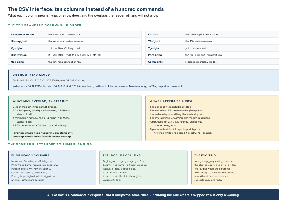
Syntax in plain English. Writing takes a file name; reading takes a list of file names. Both accept a map file if your column headings are not the standard ones.
# Write the whole bump and TSV floorplan out.
icc2_shell> write_design_io -file_name nimbus_bump_tsv.csv
icc2_shell> sh head -4 nimbus_bump_tsv.csv
Reference_name,C4_inst,Ubump_inst,TSV_inst,X_origin,Y_origin,
  Orientation,Port_name,Net_name,Comments
C4_BUMP,nim_C4_SIG_0_0,,,125,75,R0,,nim_C4_SIG_0_0_net,
C4_BUMP,nim_C4_SIG_0_1,,,275,75,R0,,nim_C4_SIG_0_1_net,
VIA_TSV,,,TSV_nim_C4_SIG_0_0,125,75,R0,,,
The file has a header row and a row of data for each cell instance. The header row is required and describes the keyword for each column. After it, each row describes a cell instance or a connection: cell rows specify the instance name, reference name, location and orientation; connection rows specify connections between terminals; and port rows create a port. You can specify multiple input files and provide different fields in each, and not all fields are required for each cell instance or connection.
What the reader does with a row. Six behaviours, and it is worth reading them as a group because four of the six end in something being skipped or ignored.
- If a cell instance does not exist, the tool creates it.
- If the cell instance already exists, it is moved to the specified location.
- If the cell instance overlaps an existing instance, it is skipped.
- If a row is invalid, the tool issues a warning message and skips the row.
- If a port does not exist, the tool ignores it — unless you pass
-create_ports. - If a port or net already exists, it retains the current setting of its
port_typeornet_typeattribute — unless you name it in-poweror-ground, which set the attribute and create the port or net if it does not exist.
The overlap rules. By default the tool performs these checks when creating new cell instances: cells of the same type cannot overlap; a C4 bump can overlap an existing microbump, TSV or standard cell; a microbump can overlap an existing C4 bump, TSV or standard cell; and a TSV can overlap an existing C4 bump or microbump. That set of rules is the nominal setting of -overlap_check, and it is the default. none means no checking is done and a new object is created even if something else exists at that location. strict means no overlap with any existing cell of any type is allowed.
| Option | What it does | Worth knowing |
|---|---|---|
| -file_name_list | The input files | Required. More than one file is allowed, with different fields in each — but only one file may be given with -eco |
| -map_file | Maps your column names onto the standard ones | One comma-separated pair per line, custom name first. Cannot be given with -eco |
| -delimiter_char | The field separator | Any single character, so a file separated by exclamation marks reads fine |
| -comment_char | The comment character | Cannot be given with -eco |
| -c4_ref_name | The C4-bump reference name | For rows that do not name one |
| -tsv_ref_name | The TSV reference name | Likewise |
| -ubump_ref_name | The microbump reference name | Likewise |
| -bond_pad_def | The default bond pad definition, for rows whose Reference_name is empty | The bond-pad counterpart of the three above |
| -instance_prefix | A prefix for automatically generated instance names | For files whose rows have no instance name |
| -overlap_check | none, nominal or strict | Default nominal, which is the four-rule set above |
| -create_ports | Creates the ports named in the file if they do not exist | Without it, a port row for a port that does not exist is ignored |
| -create_bus_high_to_low | Creates bus ports from high bit to low | Only with -create_ports. The default is low to high |
| -power | Sets port_type or net_type to power for the named ports or nets | Creates them if they do not exist |
| -ground | The same, for ground | Likewise |
| -die_origin | The die origin coordinates | By default the tool uses the lower-left corner of the die as its origin |
| -die_orientation | The die orientation | R0, R90, R180, R270, MX, MXR90, MY or MYR90. Default: no rotation |
| -cell_origin_type | Whether the coordinates mean the cell's lower-left corner or its centre | Pass center for the centre. Default is the lower-left corner |
| -units | A multiplier, if the file's length unit is not the library's | The command divides the file's values by it. An integer of one or more |
| -pseudo_bumps | Reads the bump-planning form of the file | See Section 7.4.4 |
| -eco | Reads a change file produced by compare_design_io | Supports undo and redo. Errors if given a non-change file, or omitted for a change file |
| -attribute | Reads the named user attributes as extra columns | Only attributes already defined are read; undefined ones are ignored |
| -continue_on_error | Ignores rows with warnings and processes the valid ones | Applies to both bump and pseudo-bump files |
| -mark_unconnected_as_dummy | Marks objects with no net or port name as dummy | Check the result with the is_dummy attribute |
| -always_set_preferred_pin | Sets preferred_pin even where it already exists | The counterpart of assign_3d_interchip_nets -set_port_terminals all |
| -force | Creates an instance even if the row places it outside the die area | And suppresses the error that would otherwise say so. Rarely what you want |
| -verbose | Detailed output | Worth having on the first read of any new file |
| Option | What it does | Worth knowing |
|---|---|---|
| -file_name | The output file | Required |
| -file_structure | single or split | split is only for pseudo bumps and writes the regions and the pseudo bumps as two files in a directory |
| -contents | Which object types to write | c4, ubump, bond_pad, tsv or all. Omitted, the command writes all of them |
| -objects | Only the named objects | They must be C4 bumps, microbumps or TSVs |
| -within | Only the objects inside a bounding box | The quickest way to write out one corner of a large interposer |
| -columns_file | A file naming the columns to write, in order | Both limits and orders the output. The way to hand somebody a two-column file |
| -map_file | Writes your column names instead of the standard ones | The mirror of the reader's option |
| -delimiter_char | The field separator to write | Match whatever the other side reads |
| -cell_origin_type | Whether to write the lower-left corner or the centre | Pass center and the tool calculates it from the bounding box |
| -units | A multiplier for the coordinates written | The command multiplies the micron values by it. An integer of one or more |
| -pseudo_bumps | Writes the bump-planning form | See Section 7.4.4 |
| -attribute | Writes the named user attributes as extra columns | Define them with define_user_attribute first |
| -object_type_column | Whether the file carries an Object_type column | On by default. Set it false for the older column layout that names C4_inst and its siblings instead |
Verification. Write, read back into a fresh session, and write again: the two files should agree. That round trip catches unit errors, origin-convention errors and skipped rows in one step, and it is worth doing once on any new interface before trusting it.
Common mistakes. A file whose length unit is not the library's, read without -units, so every coordinate is out by a constant factor. A file whose coordinates are cell centres, read without -cell_origin_type center, so every cell is out by half its own size. And treating warnings as noise: a run that skipped forty rows is a run that placed forty fewer cells than you think.
Finding the rest. man read_design_io and man write_design_io.
7.4.4 Bump regions, pseudo bumps, and changing a plan
Purpose. Bump planning using the concepts of bump patterns, regions and pseudo bumps offers a way to rapidly develop 3DIC designs. The point is to lay out and rearrange a bump field before the cells exist — a plan you can argue about, not a placement you have to undo.
A bump region is an area with a pattern: a boundary, a pitch in each direction, an optional offset and stagger, a default shape and a default radius. A pseudo bump is one bump inside such a region, with a row and column index, an optional net and port, and its own shape and radius if it differs from the region's.
# A region, and one bump in it.
icc2_shell> create_bump_region -name hbm_plan \
   -boundary {{2900 640} {3285 1520}} -content_type bump \
   -pattern {55 55} -array_size {8 16}
icc2_shell> create_pseudo_bump -region hbm_plan -offset {0 0} \
   -shape octagon -radius 20 -net dq_0

# Write the whole plan out, and read it back in a new session.
icc2_shell> write_design_io -pseudo_bumps -file_name nimbus_plan.csv
icc2_shell> read_design_io -pseudo_bumps -file_name nimbus_plan.csv
The file has two sections with their own column sets. In the bump-region section, Name, Boundary, Pitch_X, Pitch_Y and Bump_radius are mandatory and a value is required for each. Pattern_offset_X and Pattern_offset_Y give the delta from the region's lower-left corner to the start of the pattern. Row_stagger_X and Column_stagger_Y give cyclical deltas for the start of each row or column. Orientation takes the eight rotation values and defaults to R0 when blank. Bump_shape takes triangle, square, pentagon, hexagon, septagon, octagon or circle, and defaults to octagon. Is_backside defaults to false. Port_pattern and Net_pattern hold two-dimensional patterns of port and net names.
In the pseudo-bump section: Region_name says which region the bump lives in; X_origin and Y_origin give the centre of the bump; Row and Column are index numbers starting from zero; Net_name and Port_name give the connections; Shape and Radius override the region's defaults; and Is_hole, Is_probe_pad, Is_dummy and Is_default are true-or-false flags that default to false.
Why does a pseudo bump have a shape from a list of seven polygons? Because a bump-planning discussion is about clearances, and a clearance depends on the outline. An octagon is the usual approximation of a round bump because it is cheap to test against; a square is used where the process actually produces one; and the odd entries in the list — a triangle, a septagon — exist because somebody's process needed them. The default is octagon, and if you do not have a reason to change it, do not.
Adding a column of your own. To carry an attribute the standard columns do not cover, define it first, then name it when you write and again when you read. The attribute can be Boolean, double, float, int or string, and for a string type the value must not contain a comma — which is the sort of restriction that is obvious once stated and unfindable at three in the afternoon.
# Define, write, and in a new session define again before reading.
icc2_shell> define_user_attribute -type string -classes cell \
   -name owner_team
icc2_shell> write_design_io -file_name nimbus_plan.csv \
   -attribute {owner_team}
icc2_shell> read_design_io -file_name nimbus_plan.csv \
   -attribute {owner_team}
The tool reads only those user attributes that are defined; if an attribute is undefined it is ignored. So the definition has to be repeated in the reading session, and a plan file carrying a column nobody has defined loses that column silently.
Changing a plan. Three commands, in order. compare_design_io takes two files with the I/O elements of two versions of a design, compares them and generates the differences, either shown in the graphical interface as a table or written to a file. read_design_io -eco then reads that difference file.
# Compare two versions of the plan, and apply the difference.
icc2_shell> compare_design_io -pseudo_bumps -golden nimbus_plan_v1.csv \
   -v2 nimbus_plan_v2.csv -output nimbus_plan_eco.csv
icc2_shell> read_design_io -pseudo_bumps -eco \
   -file_name nimbus_plan_eco.csv
Four rules govern the change flow. Only one change file can be specified. There must be a current design when the command runs. The read supports undo and redo. And three options cannot be combined with -eco: -map_file, -comment_char and -units. Giving -eco a file that is not a change file, or omitting -eco for a file that is, produces an error either way.
7.4.5 The interposer power mesh
Purpose. The interposer mounts the active die and connects them, and in addition to signals, power and ground are routed through it to power the die. To provide adequate power and minimise voltage drop, you build a mesh inside the interposer to distribute power from the package to the die.
The path is worth stating once, because it explains the whole structure: interposers connect to the package through C4 bumps on the back side, then distribute power to the microbumps on the front side, which connect to the flip-chip bumps on the die. A mesh on the intermediate routing layers helps minimise the voltage drop the extra routing would otherwise cause.
Syntax in plain English. Standard power-planning commands, used on an unusual object. Define a pattern; associate it with a region and a pair of nets; compile.
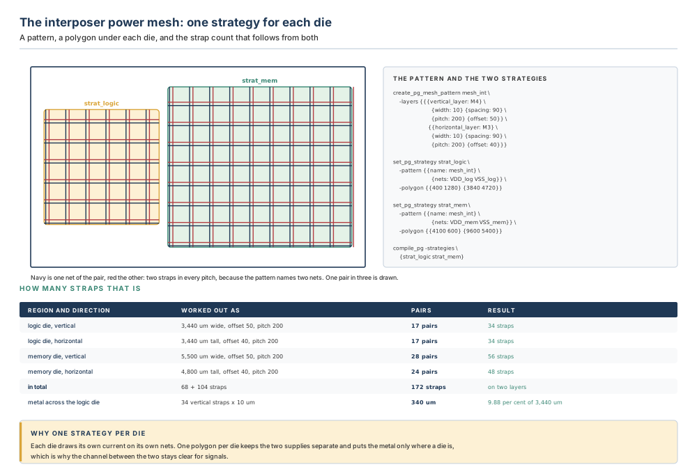
# 1. The pattern: two layers, two nets, and four numbers each.
icc2_shell> create_pg_mesh_pattern mesh_int \
   -layers {{{vertical_layer: M4} {width: 10} {spacing: 90} \
             {pitch: 200} {offset: 50}} \
            {{horizontal_layer: M3} {width: 10} {spacing: 90} \
             {pitch: 200} {offset: 40}}}

# 2. One strategy per die, over that die's own footprint.
icc2_shell> set_pg_strategy strat_logic \
   -pattern {{name: mesh_int} {nets: VDD_log VSS_log}} \
   -polygon {{400 1280} {3840 4720}}
icc2_shell> set_pg_strategy strat_mem \
   -pattern {{name: mesh_int} {nets: VDD_mem VSS_mem}} \
   -polygon {{4100 600} {9600 5400}}

# 3. Compile both.
icc2_shell> compile_pg -strategies {strat_logic strat_mem}
Reading the pattern's four numbers. A width of 10 and a spacing of 90 put the two straps of a pair 100 µm apart, centre to centre of their gap. A pitch of 200 puts the next pair 200 µm after the first. An offset of 50 starts the first pair 50 µm inside the region. Two nets in the strategy means two straps per pitch — one per net — so a 200 µm pitch over a 3,440 µm die gives seventeen pairs and therefore thirty-four straps.
# The logic die's polygon, vertical direction.
region        400 to 3,840 um, so 3,440 um wide
first pair    400 + 50 = 450 um
pair spacing  200 um
last pair     450 + 16 x 200 = 3,650, and its second strap at 3,750
              which is inside 3,840 - 10, so 17 pairs fit
straps        17 x 2 = 34

# Checked the other way: metal used.
metal         34 x 10 = 340 um of 3,440 = 9.88 per cent
Prerequisites. Every die placed, so its footprint is a polygon. And the polygon has to be the die's real footprint: {{400 1280} {3840 4720}} is the logic die's placement plus its size, and getting it from the placement rather than typing it is how it stays right when the die moves.
Expected result. A mesh beneath each die, on the two named layers, on that die's own nets. On Nimbus-8 that is 172 straps in total: 68 under the logic die and 104 under the memory die.
Verification. Count the straps and compare with the arithmetic. Then look at the channel between the die: if the mesh has spilled into it, one of the polygons is wrong, and the channel is where the die-to-die signals have to run.
Common mistakes. One strategy over the whole interposer, which puts power metal in the channel and shorts the two die's supplies onto one pair of nets. A polygon typed by hand and then not updated when a die moved. And forgetting that the step exists at all: an interposer with no mesh routes and passes every check in this chapter, and fails in an analysis nobody in this chapter runs.
Finding the rest. man create_pg_mesh_pattern, man set_pg_strategy and man compile_pg. Chapter 10 treats power planning properly; this is the interposer-shaped corner of it.
7.4.6 Routing the interposer, and the channel arithmetic that comes first
Purpose. After the bumps are placed, the TSVs created and the power grid built beneath the die, the interposer can be routed. Three methods are supported: routing with Zroute, routing with the redistribution-layer router, and combining both.
But first, the arithmetic. This is the part of the chapter with no command in it, and it is the part that decides whether the rest works.
Nimbus-8's logic die and memory stack exchange 128 signals. The interposer has two redistribution layers available for them. The routing rule gives each route a width of 2 µm and a spacing of 2 µm, so a track occupies 4 µm. The question is how wide the gap between the two die has to be.
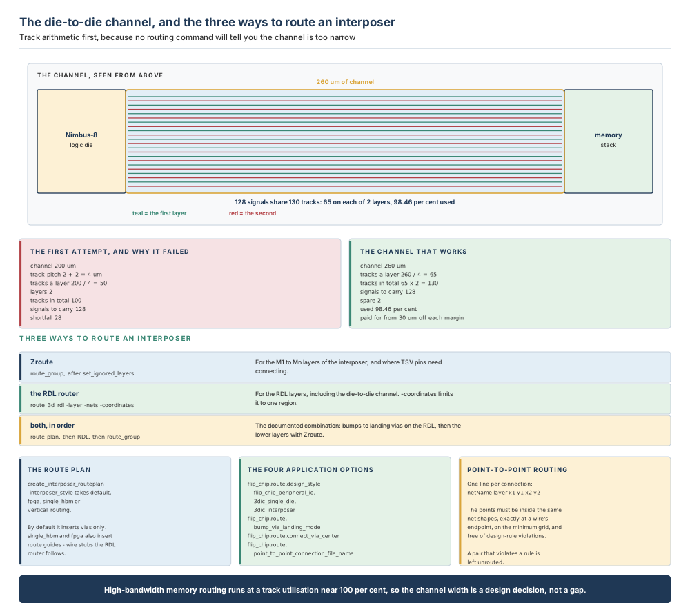
# First attempt: the gap the outline happened to leave.
channel                200 um
track pitch            2 + 2 = 4 um
tracks a layer         200 / 4 = 50
layers                 2
tracks in total        50 x 2 = 100
signals to carry       128
shortfall              28

# What the signals actually need.
tracks a layer         128 / 2 = 64
channel                64 x 4 = 256 um, rounded up to 260
tracks a layer         260 / 4 = 65
tracks in total        65 x 2 = 130
spare                  130 - 128 = 2
used                   128 / 130 = 98.46 per cent
paid for from          (260 - 200) / 2 = 30 um off each margin
Sixty microns is not much. But it is sixty microns that had to come from somewhere, and the somewhere was the margin between each die and the interposer edge, which went from 430 µm to 400. Had the interposer outline already been fixed with the dies at their original spacing, those sixty microns would have had to come out of the interposer, and the interposer size is a package decision.
Interposer designs that incorporate high-bandwidth memory have physical design requirements more stringent than other interposer configurations: high-density routing, often with track utilisation nearing 100 per cent; a limited number of routing layers, often two; highly parallel bus routing; length matching for critical data signals; and coaxial shielding.
Read that list as a warning about slack. A design running at 98.46 per cent track utilisation has two spare tracks in the whole channel. Add one signal and the channel is full; add three and it does not fit. There is no version of this problem that gets easier later, which is why the arithmetic belongs on the first page of the plan rather than in the routing step.
The route plan. When routing an interposer for high-bandwidth memory you want finer control over where the vias and nets go, and create_interposer_routeplan provides it. The command analyses an interposer containing pre-placed and pre-assigned front-side and, optionally, back-side bumps; based on their configuration it creates and places vias connecting the bumps to a second layer for routing, and creates routing guidance in the form of wire-stub pre-routes called route guides. It also routes the centre section between the bump arrays. The placed bump vias and the route guides together are the route plan.
-interposer_style takes default, fpga, single_hbm or vertical_routing. By default the command inserts vias only; to insert vias and route guides, specify single_hbm or fpga. The tool processes different types of pattern file depending on the style, and -pattern_file names the file. The pattern file is an ASCII file of one or more sections, each beginning with a keyword followed by constraints inside curly brackets, and the tool uses a default file unless you supply one.
# Set the design style, then create the plan.
icc2_shell> set_app_options -name flip_chip.route.design_style \
   -value 3dic_interposer
icc2_shell> create_interposer_routeplan -interposer_style single_hbm \
   -pattern_file nimbus_hbm.pat
icc2_shell> set_attribute [get_vias *] shape_use user_route
That last line matters more than it looks. Setting the shape type of the pre-placed vias to user_route preserves them until the routing stage; without it, a later step is free to remove work the route plan just did.
Routing the channel. With the plan in place, the rules and the nets:
# The rule, for the channel's two layers.
icc2_shell> create_routing_rule rdl_chan \
   -widths {MRDL 2 M9 2} -spacings {MRDL 2 M9 2}
icc2_shell> set_routing_rule [get_nets $chan_nets] -rule rdl_chan

# Bumps to their landing vias first.
icc2_shell> set_app_options \
   -name flip_chip.route.bump_via_landing_mode -value true
icc2_shell> route_3d_rdl -nets [get_nets $chan_nets] -layer MRDL \
   -coordinates {{3840 600} {4100 5400}}

# Then the via-to-stub nets, with the point-to-point file the
# route plan produced.
icc2_shell> set_app_options \
   -name flip_chip.route.bump_via_landing_mode -value false
icc2_shell> set_app_options \
   -name flip_chip.route.point_to_point_connection_file_name \
   -value nimbus_p2p.txtM9
icc2_shell> route_3d_rdl -nets [get_nets $chan_nets] -layer M9 \
   -coordinates {{3840 600} {4100 5400}}
The -coordinates option takes a list of rectangles and speeds routing up by routing inside them only. On this design the rectangle is the channel: {{3840 600} {4100 5400}} is exactly the 260 µm gap, from the logic die's right edge to the memory die's left, spanning the memory die's height.
Point-to-point routing. After routing bumps to landing vias you can specify point-to-point connections between bumps, landing vias and wire stubs, by providing a line per connection in a route plan file: a net name, a layer, and two points. Four requirements apply to the points. They must fall inside the same net shapes — a wire, a via or a pin shape. For wire shapes the point must be exactly at the endpoint of the wire, although the router does not necessarily connect to pins and vias exactly at the point specified. They must be on the minimum grid. And they must be on coordinates that do not have design-rule violations, meaning that routing a wire to the specified point creates no violation with neighbouring shapes. Routing pairs with violations are left unrouted.
| Command or option | What it does | Worth knowing |
|---|---|---|
| create_interposer_routeplan | Creates the bump vias and, in some styles, the route guides | -interposer_style takes default, fpga, single_hbm or vertical_routing |
| create_interposer_routeplan -pattern_file | Names the pattern file of constraints and directives | A default file is used if you supply none. The style decides which kind of file is expected |
| route_3d_rdl -layer | Routes the RDL nets on one layer | -layer is required. -nets or -nets_in_file chooses the nets |
| route_3d_rdl -coordinates | Routes inside a list of rectangles only | The way to route a channel without touching the rest of the interposer |
| route_3d_rdl -skip_detail_route | Global routing only | Pairs with -reuse_existing_global_route, which does detail routing on an existing global route |
| route_group -nets | Routes the named nets with Zroute | For the interposer's lower metal layers |
| set_ignored_layers | Narrows the layer range Zroute may use | -min_routing_layer and -max_routing_layer, and front-side and back-side variants of both |
| create_routing_rule | Widths, spacings, and the shield widths and spacings | Also -rdl_taper_distances and -rdl_taper_widths for a tapered route |
| create_rdl_shields | Creates the shields | Side-wall by default; coaxial with -reference_layer and -offset. -coordinates restricts it to a region |
| flip_chip.route.design_style | The design style, set before using the RDL commands | Documented values flip_chip_peripheral_io, 3dic_single_die and 3dic_interposer. Read it back rather than assume it |
| flip_chip.route.bump_via_landing_mode | Whether the router connects each bump to the nearest interlayer via | Set true for the bump-to-via pass, false for the via-to-stub pass. Read it back rather than assume the default |
| flip_chip.route.connect_via_center | How the RDL router connects RDL routes to vias | Set deliberately in the documented high-bandwidth flow |
| flip_chip.route.point_to_point_connection_file_name | The point-to-point connection file for the RDL commands | Set once per layer, before each route_3d_rdl pass on that layer |
| flip_chip.route.shielding_net | The net the shields connect to | Set it before creating the shield rule |
| shape_use user_route | An attribute, not an option: preserves pre-placed vias | Set on the vias the route plan created, or a later step may remove them |
The combined flow is worth knowing as a shape rather than a script. Create the route plan in the default mode, which inserts vias. Preserve those vias with shape_use user_route. Create a wide routing rule and apply it. Route the bumps to their landing vias on the RDL layer with bump_via_landing_mode true, then set it false. Narrow the layer range with set_ignored_layers and route the lower layers with route_group. And if the design has back-side layers, route those with route_3d_rdl on the back-side layer.
Six steps, four of which set something up. That ratio is normal for interposer routing and it is why the pattern file and the application options are worth reading back rather than trusting.
Verification. report_rdl_routes -open_nets true for the opens, and report_rdl_routes -create_error_data verification to write an error database covering opens and shorts. Then the connectivity category of check_3d_design.
Common mistakes. Routing before the channel arithmetic, and discovering the shortfall as congestion. Omitting -coordinates on a channel route, so the router works on the whole interposer and takes an hour to tell you the same thing. Leaving bump_via_landing_mode true for the second pass, so the via-to-stub routing behaves like the bump-to-via routing. And forgetting shape_use user_route, which is invisible until the vias are gone.
7.4.7 check_3d_design — ten categories, all on by default
Purpose. Validate the whole system. In a 3DIC design, multiple chips are stacked vertically or placed side by side on an interposer; at the top level the entire stack is modelled as a virtual top-level design and the individual chips as cells. This command checks that model.
The one thing to know before anything else. The command should be used at the last step of the 3DIC design flow, and run at the top level. And unlike Chapter 6's check_io_placement, running it with no options performs all the checks.
# Everything, which is the default.
icc2_shell> check_3d_design

# Or one category, when you are iterating on that category.
icc2_shell> check_3d_design -chip_placement

# Or everything except one, when a category is not ready yet.
icc2_shell> check_3d_design -exclude {pg}
| Category | What it checks |
|---|---|
| -chip_placement | The vertical level and overlap of the top-level chips. Two chips with the same z value must not overlap. Where two chips are neighbouring, the one with the larger virtual top-level area should contain the other. |
| -physical_contact | Physically contacted bumps: non-aligned bump pairs, bumps that do not physically connect to a bump on the adjacent side of a vertical neighbour, bumps that contact more than one bump of a neighbour, and a bump overlapping another bump within a single chip. |
| -logical_physical_consistency | Whether every top-level port instance pair has a corresponding physical bump pair. If it does not, the command issues an error. |
| -connectivity | The connectivity of the design. |
| -matching_type | Matching type mismatches on logical connection and physical contact among all die in the design. |
| -bump_cluster | That a bump cluster in a chip has no more than one net, and that if one bump of a physical contact pair belongs to a cluster, the other belongs to a cluster too. |
| -physical_design_rule | TSV-to-TSV spacing against the technology file's minCutSpacing, and TSV-to-cell-boundary spacing against its tsvKeepoutSpacing. |
| -power | Power and ground net continuity. Named pg in the -exclude list, which is the one naming inconsistency to remember. |
| -tech_files | Whether the technology files in the design differ, and detects multiple technology files inside a single die, which is invalid. |
| -feedthrough | Whether any chip needs to punch new ports during the assign or propagate of top nets. |
The options that are not checks. -dies, -die_pairs and -exclude_dies narrow which die the violations are shown for, and each expands a hierarchy die into its leaf die. -no_probe_pad hides violations involving probe pads. -verbose prints the detail; without it the command prints only part of the messages and a summary. -error_view names the file for the graphical error browser, defaulting to check3dDesign.err. -group_by_id reports by message identifier. -exclude takes a category list and must not be given together with the category options themselves. And -flyline_analysis takes all, signal or pg and writes a net-based flyline report of total length, crossings and dangling or out-of-box sources — and when it is used, all other checking items are disabled.
Prerequisites. The command's own page lists four: create_3d_mirror_bumps, propagate_3d_connections, propagate_3d_matching_types and set_cell_location. That list is the honest reason the command belongs at the end: three of the four are step-three commands, and running the check before them means checking a system that does not exist yet.
Expected result. Warning and error messages that indicate potential problems, which might need correcting before manufacturing. The full list of conditions it looks for runs to more than twenty items, and reading it once is worth the ten minutes — it is the most complete statement anywhere of what a valid 3DIC assembly is.
Common mistakes. Running it early, which is the misleading one and gets its own row in Table 7.11. Giving -exclude alongside a category option, which is not allowed. Using -flyline_analysis and reading the clean result as a pass, when every other check was disabled. And reading “0” without -verbose: the command prints only part of the messages otherwise.
Finding the rest. man check_3d_design, and then the man page for each error message it reports, which is where the guidance for fixing each one lives.
-flyline_analysis quietly turns all of it off.7.5 The worked example: Nimbus-8 becomes a 2.5D system
Ten steps, in the order Figure 7.4 gave them, starting from the die Chapter 6 finished. Every number has appeared already; this is where they are produced rather than quoted.
Step 0 — the arithmetic, on paper, before the first command
# What we were given, and by whom.
logic die     = 3,440 um on each side       (Chapter 4, then Chapter 6)
memory die    = 5,500 x 4,800 um            (the memory vendor)
interposer    = 10,000 x 6,000 um           (the package)
C4 pitch      = 150 um                      (the package)
microbump pitch = 55 um                     (the attach process)
die-to-die signals = 128, on 2 RDL layers   (the memory interface)
RDL width/spacing  = 2 um / 2 um            (the interposer technology)
library scale factors = 4,000 / 10,000 / 2,000

# The session scale factor, first, because nothing runs without it.
lcm(4,000, 10,000, 2,000) = 20,000
check: 20,000 / 4,000 = 5, / 10,000 = 2, / 2,000 = 10  -> all whole

# The channel. Two attempts.
track pitch    = 2 + 2 = 4 um
attempt 1      200 um gap -> 200 / 4 = 50 a layer x 2 = 100 tracks
               128 signals - 100 = 28 short: rejected
attempt 2      128 / 2 = 64 a layer -> 64 x 4 = 256, round up to 260
               260 / 4 = 65 a layer x 2 = 130 tracks
               130 - 128 = 2 spare, 128 / 130 = 98.46 per cent used

# Which fixes every placement number on the interposer.
margin each side = (10,000 - (3,440 + 260 + 5,500)) / 2 = 400 um
logic die at     (400, (6,000 - 3,440) / 2) = (400, 1,280)
memory die at    (400 + 3,440 + 260, (6,000 - 4,800) / 2) = (4,100, 600)
check            400 + 3,440 + 260 + 5,500 + 400 = 10,000
Check each figure backwards before it goes anywhere. 1,280 + 3,440 + 1,280 = 6,000, and 600 + 4,800 + 600 = 6,000, so both die are vertically centred. 4,100 + 5,500 = 9,600, and 10,000 − 9,600 = 400, so the two margins agree. And the two die areas, 11.8336 mm² and 26.40 mm², sum to 38.2336 mm² = 38,233,600 µm², which is 63.72 per cent of the interposer's 60.00 mm² = 60,000,000 µm², leaving 21.7664 mm² — 36.28 per cent — of interposer with no die on it.
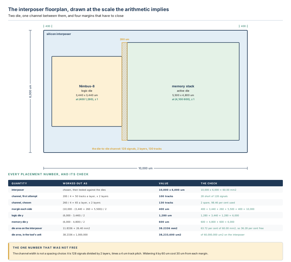
Thirty-six per cent of a centimetre-square piece of silicon with nothing on top of it looks wasteful, and somebody will say so. It is not: that area is where the C4 bumps go, where the die-to-die routes turn, and where the mesh reaches out from under one die towards the other. An interposer covered edge to edge in die has nowhere to put its own wiring.
Step 1 — prepare each active die
# The logic die: Chapter 6's netlist and floorplan, a new bump field.
icc2_shell> set_app_options -name design.session_scale_factor \
   -value 20000
icc2_shell> read_verilog nimbus_logic.v
icc2_shell> read_def nimbus_logic.def

# The channel band, facing the memory die.
icc2_shell> create_bump_array -lib_cell UBUMP -name ub_chan \
   -delta {55 55} -repeat {8 16} \
   -bbox {{2900 640} {3285 1520}}

# The package band, facing the other way.
icc2_shell> create_bump_array -lib_cell UBUMP -name ub_pkg \
   -delta {55 55} -repeat {4 16} \
   -bbox {{155 640} {320 1520}}

# The power and ground field, in the middle.
icc2_shell> create_bump_array -lib_cell UBUMP -name ub_pg \
   -delta {55 55} -repeat {15 15} -pattern staggered_1 \
   -bbox {{1335 1335} {2105 2105}}
# Where those three shapes come from.
sites across the die   3,440 / 55 = 62 sites
                       61 x 55 = 3,355, so 42.5 um each edge
signal microbumps      channel band  8 x 16 = 128
                       package band  4 x 16 =  64
                       total                = 192
power microbumps       15 x 15 staggered_1, 8x8 + 7x7 = 113
logic die total        192 + 113 = 305

# And the check that it was done honestly.
Chapter 6 gave this die 305 bumps. It still has 305.
That last line is the whole point of the step. The pitch changed from 150 µm to 55 µm and the arrangement changed from four peripheral bands plus a central field to two bands plus a central field, but the count did not, because the count came from the netlist and the power budget rather than from the geometry. If a rearrangement changes the count, something was dropped.
The memory die is prepared the same way and arrives with 128 channel microbumps — matching the logic die's channel band exactly — plus a 12 × 12 staggered field giving 6 × 6 + 6 × 6 = 72 power and ground microbumps, for 200 in total.
Step 2 — the interposer
icc2_shell> create_lib nimbus_interposer.ndm \
   -technology interposer.tf \
   -ref_libs {c4_bump.nlib front_ubump.nlib physicalonly.nlib}
icc2_shell> read_verilog interposer.v
icc2_shell> initialize_floorplan -control_type die \
   -boundary {{0 0} {10000 6000}}
# C4 bumps, on the back side, at the package's pitch.
# The signal band first: 64 of them, one per package signal.
icc2_shell> create_bump_array -lib_cell C4_BUMP -name c4_sig \
   -delta {150 150} -repeat {8 8} -origin {125 75}

# Then a power field under each die.
icc2_shell> create_bump_array -lib_cell C4_BUMP -name c4_pg_log \
   -delta {150 150} -repeat {8 8} -origin {875 1875}
icc2_shell> create_bump_array -lib_cell C4_BUMP -name c4_pg_mem \
   -delta {150 150} -repeat {6 6} -origin {5675 1875}

# One TSV per C4 bump. Every one of them.
icc2_shell> derive_3d_interface -from [get_cells c4_*] \
   -to_object_ref [get_via_defs -tech [get_techs *] VIA_TSV] \
   -name_prefix TSV_c4
icc2_shell> create_matching_type \
   -name Signal [all_connected [get_nets *SIG*]]
# The back-side arithmetic.
C4 sites across   10,000 / 150 = 66,  65 x 150 = 9,750, margin 125 um
C4 sites up        6,000 / 150 = 40,  39 x 150 = 5,850, margin  75 um
inline sites      66 x 40 = 2,640
C4 bumps placed   64 signal + 64 + 36 power = 164
site use          164 / 2,640 = 6.21 per cent
TSVs created      164, one per C4 bump

# The contrast that explains the interposer.
front side  505 microbumps at  55 um pitch
back side   164 C4 bumps   at 150 um pitch
ratio       505 / 164 = 3.08 to 1, against a pitch ratio of 2.727 to 1
Six per cent site use on the back side, against Chapter 6's 63.02 per cent on the die. That is not slack — it is what a 150 µm pitch looks like on a piece of silicon a centimetre wide, and it is the reason the interposer exists.
Step 3 — the top-level design
icc2_shell> create_lib nimbus_top.ndm -technology top.tf \
   -ref_libs {nimbus_logic.ndm nimbus_mem.ndm nimbus_interposer.ndm}
icc2_shell> read_verilog nimbus_top.v
icc2_shell> initialize_floorplan -boundary {{0 0} {10000 6000}}
icc2_shell> set_attribute [current_block] design_type 3dic

icc2_shell> set_cell_location interposer_inst \
   -coordinates {0 0} -z_offset 0 -orientation N
icc2_shell> set_cell_location logic_die_inst \
   -coordinates {400 1280} -z_offset 1 -orientation FN
icc2_shell> set_cell_location mem_die_inst \
   -coordinates {4100 600} -z_offset 1 -orientation FN

icc2_shell> report_3d_chip_placement -chips \
   {logic_die_inst mem_die_inst interposer_inst}
chip_name        design_type  stack_z  location      orientation  scaling_factor
logic_die_inst   die          1        (400 1280)    FN           1
mem_die_inst     die          1        (4100 600)    FN           1
interposer_inst  die          0        (0 0)         N            1

icc2_shell> check_3d_design -chip_placement
That last line is the one exception to “run the check at the end”, and it is a deliberate one: -chip_placement is the only category whose prerequisites are satisfied at this point, since it depends on nothing but set_cell_location. Running it here catches an overlap or a z value that does not start at zero while the fix is still one command.
Step 4 — mirror the microbumps
icc2_shell> save_block
icc2_shell> save_lib
icc2_shell> close_lib
icc2_shell> open_lib nimbus_top.ndm -ref_libs_for_edit
icc2_shell> set_editability \
   -blocks nimbus_interposer.ndm:interposer.design

icc2_shell> create_3d_mirror_bumps -from logic_die_inst \
   -to interposer_inst -ref_cell UBUMP -prefix logic \
   -use_port_names
icc2_shell> create_3d_mirror_bumps -from mem_die_inst \
   -to interposer_inst -ref_cell UBUMP -prefix mem \
   -use_port_names
# Count them, because the count is the check.
logic 305 + memory 200 = 505 microbumps on the interposer front side
get_cells logic*  -> 305
get_cells mem*    -> 200
Step 5 — connect, match and assign
icc2_shell> propagate_3d_connections

icc2_shell> current_design interposer
icc2_shell> add_to_matching_type Signal [get_cells logic_dq* mem_dq*]
icc2_shell> create_matching_type -name Power \
   [get_pins *VDD_log*/PAD *VDD_mem*/PAD]
icc2_shell> create_matching_type -name Ground \
   [get_pins *VSS_log*/PAD *VSS_mem*/PAD]

icc2_shell> current_design nimbus_top
icc2_shell> propagate_3d_matching_types
icc2_shell> assign_3d_interchip_nets -include_pg_nets \
   -set_port_terminals incremental
Two options on that last command are decisions, not defaults. -include_pg_nets is there because the power and ground bumps have to be assigned too and are excluded otherwise. -set_port_terminals incremental is there because the channel nets each reach more than one bump, and without it the ambiguity is resolved silently — with it, the choice is recorded in the preferred_pin attribute where a reviewer can read it.
Step 6 — the virtual interface blocks
icc2_shell> create_3d_virtual_blocks -in_netlist
Two blocks, because there are two adjacent die pairs: the logic die against the interposer, and the memory die against the interposer. The two active die are at the same z level and face each other edge-on rather than face-to-face, so no block is created between them.
Step 7 — the power mesh
icc2_shell> create_pg_mesh_pattern mesh_int \
   -layers {{{vertical_layer: M4} {width: 10} {spacing: 90} \
             {pitch: 200} {offset: 50}} \
            {{horizontal_layer: M3} {width: 10} {spacing: 90} \
             {pitch: 200} {offset: 40}}}
icc2_shell> set_pg_strategy strat_logic \
   -pattern {{name: mesh_int} {nets: VDD_log VSS_log}} \
   -polygon {{400 1280} {3840 4720}}
icc2_shell> set_pg_strategy strat_mem \
   -pattern {{name: mesh_int} {nets: VDD_mem VSS_mem}} \
   -polygon {{4100 600} {9600 5400}}
icc2_shell> compile_pg -strategies {strat_logic strat_mem}
# The straps, counted before and after.
logic die   3,440 um each way, 17 pairs each way -> 68 straps
memory die  5,500 um wide, 28 pairs             -> 56 straps
            4,800 um tall, 24 pairs             -> 48 straps
total       68 + 104 = 172 straps on two layers
metal       34 x 10 = 340 um of 3,440 = 9.88 per cent of the logic die
Step 8 — route the channel, then the rest
icc2_shell> set_app_options -name flip_chip.route.design_style \
   -value 3dic_interposer
icc2_shell> report_app_options flip_chip.route.design_style

icc2_shell> create_interposer_routeplan -interposer_style single_hbm \
   -pattern_file nimbus_hbm.pat
icc2_shell> set_attribute [get_vias *] shape_use user_route

icc2_shell> create_routing_rule rdl_chan \
   -widths {MRDL 2 M9 2} -spacings {MRDL 2 M9 2}
icc2_shell> set_routing_rule [get_nets $chan_nets] -rule rdl_chan

icc2_shell> set_app_options \
   -name flip_chip.route.bump_via_landing_mode -value true
icc2_shell> route_3d_rdl -nets [get_nets $chan_nets] -layer MRDL \
   -coordinates {{3840 600} {4100 5400}}
icc2_shell> set_app_options \
   -name flip_chip.route.bump_via_landing_mode -value false
icc2_shell> route_3d_rdl -nets [get_nets $chan_nets] -layer M9 \
   -coordinates {{3840 600} {4100 5400}}

icc2_shell> set_ignored_layers -min_routing_layer M1 \
   -max_routing_layer M4
icc2_shell> route_group -nets [get_nets $pkg_nets]
icc2_shell> report_rdl_routes -open_nets true
The rectangle in -coordinates is the channel and nothing else: {{3840 600} {4100 5400}} is 3,840 (the logic die's right edge, 400 + 3,440) to 4,100 (the memory die's left edge), spanning 600 to 5,400 (the memory die's height). Restricting the router to it is the difference between a two-minute run and a two-hour one.
Step 9 — check the whole system
icc2_shell> check_3d_design -verbose -error_view nimbus_3d.err
No category options, because all ten are wanted. -verbose, because without it the command prints only part of the messages and a summary. And an error view name, because the next person to look at this will want the browser rather than the log.
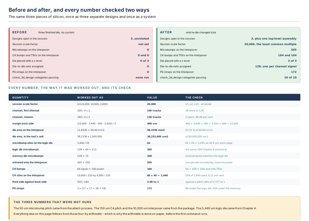
Engineering judgement — the five calls that were not the tool's to make
Two hundred and sixty microns, not two hundred. The gap the two die happened to leave was 200 µm and it held 100 tracks for 128 signals. The fix cost 60 µm of channel, taken 30 µm from each margin. Nothing in the flow raises this; the routing step would simply have failed to route 28 nets, three weeks later, after the interposer outline had been agreed.
Two spare tracks, not twenty. Having widened the channel, 300 µm would have given 150 tracks and 22 spare. It was not chosen, because the margin those 40 microns came from is what the C4 bumps and the mesh reach-out need. Ninety-eight per cent utilisation is uncomfortable, and it is what the reference says these designs run at. The defensible position is not “98 per cent is fine” but “the alternative was worse, and here is the arithmetic”.
Rearranging the logic die's bumps rather than keeping Chapter 6's field. The 150 µm field was designed for a package. Keeping it would have meant an interposer whose microbumps sat at 150 µm — legal, and a waste of the attach process. The count stayed at 305 and the area shrank by roughly a factor of seven. This is the one step in the chapter that changes an earlier chapter's output, and it is worth saying out loud in a review rather than letting somebody discover it.
-set_port_terminals incremental, not all and not omitted. Omitted, the ambiguity is resolved without a record. all resets every preferred pin on every run, so two runs can differ. incremental records a choice once and leaves it alone, which is the behaviour you want from something a reviewer may have already signed off.
Running -chip_placement early, and nothing else. The check belongs at the end of the flow. One of its ten categories depends only on set_cell_location, so running that one alone after step 3 is free information. Running the whole command there is not: it would report nine categories' worth of errors about work not yet done, and the honest response to a report like that is to stop reading it.
7.6 Failure modes and how to recognise them
Twelve ways this goes wrong. Three produce no message at all, one ends the session outright, and one produces so many messages that the right response is to ignore all of them.
| # | What went wrong | How you notice | What to do |
|---|---|---|---|
| 1 | The session scale factor was not set, or is not a multiple of every library's. | The session ends. Opening a library with a different scale factor makes the command issue an error message and exit. This is the loudest failure in the book. | Collect all three factors, compute the least common multiple, and set the option in the first ten lines of the setup script with the arithmetic in a comment. |
| 2 | A half-node library's half_node_scale_factor is set but design.is_3dic_mode is not true. | Nothing. The library reads at the wrong size, and nothing about a coordinate says what it was supposed to be. | Set the application option on the top design and read it back with report_app_options. Then check one known dimension in the library against its datasheet. |
| 3 | The channel between the die is too narrow for the signals it must carry. | Congestion, then unrouted nets, at the routing step — long after the interposer outline was agreed with the package. | Do the arithmetic in Section 7.4.6 before the outline is agreed. Signals divided by layers, times the track pitch, is the minimum width. |
| 4 | The two die's facing microbump bands have different counts or different pitches. | The physical-contact check reports non-aligned bump pairs, or bumps that do not physically connect to a bump on the adjacent side. | Compare the two counts on paper at handover. Both bands are somebody else's deliverable, and neither owner can see the other's. |
| 5 | New C4 bumps were added and derive_3d_interface was not re-run. | Nothing, until the very end. The new bumps have no TSV, so they connect to nothing, and only the connectivity check notices. | Re-run the derive step after any change to the bump field, and compare the bump count with the TSV count. They are equal or something is wrong. |
| 6 | create_3d_mirror_bumps was run before the block was made editable. | A failure. This is the friendly kind of mistake: the command does not do half the job. | open_lib -ref_libs_for_edit, then set_editability on each block, then mirror. |
| 7 | The mirror was run before the die's bump field was final. | Nothing at the time. Later, the interposer's microbumps do not match the die they were copied from, because the die changed. | Treat the die's bump field as a frozen deliverable with a revision, and record which revision the mirror was taken from. |
| 8 | assign_3d_interchip_nets was run without -include_pg_nets. | The signal nets assign and the power and ground bumps do not. The command's own output looks like a success, because it counts what it did. | Pass -include_pg_nets deliberately, and count the assigned nets against the nets you expected — not against the command's own total. |
| 9 | One power strategy was written for the whole interposer instead of one per die. | Power metal in the die-to-die channel, and both die's supplies on one pair of nets. The mesh looks fine in isolation. | One set_pg_strategy per die, each with a -polygon taken from that die's placement, each with that die's own nets. |
| 10 | The route plan's vias were not preserved with shape_use user_route. | The vias are gone by the time you route, and the route guides lead nowhere. | Set the attribute immediately after create_interposer_routeplan, in the same block of the script, so the two are never separated. |
| 11 | check_3d_design was run with -flyline_analysis. | A flyline report and nothing else. When that option is used, all other checking items are disabled — so the run is clean because it checked nothing else. | Run the flyline analysis as its own command, on purpose, and never as part of the sign-off run. Then run check_3d_design with no options at all. |
| 12 | check_3d_design was run at step 3 instead of step 9. | Hundreds of errors, almost all of them correct. This is the misleading one: the report is accurate and useless, and the natural response is to stop believing the command. | Run only -chip_placement early, since it is the one category whose prerequisites are met. Save the rest for the last step, at the top level, as the command's own page says. |
Rows 2, 5, 7 and 8 are the same failure wearing four coats, and it is the pattern this book has been tracking since Chapter 2: absence reported as success. A library at the wrong scale, a bump with no via, a copy of a stale original, a class of net nobody assigned — in every case the command that should have said something is a command nobody ran, and the commands that did run reported honestly on the smaller job they were given.
This chapter adds a fifth coat, and it is new: too much information reported as success. Row 12 produces hundreds of true errors, and row 11 produces a clean report by disabling the checks. Both end the same way — with an engineer who has stopped reading the output. The habit that catches all six variations is unchanged: after a check passes, confirm it examined what you think it examined. The addition for this chapter is its converse: after a check fails at scale, confirm it was asked at a moment when it could have passed.
7.7 Hands-on mini lab
A new system, Carina-4, on the same shape of problem with different numbers. Do the arithmetic on paper before you write a command; that is the whole exercise.
| Item | Value |
|---|---|
| Interposer, from the package | 12,000 × 7,000 µm |
| Logic die | A square 4,000 µm on each side |
| Memory die, from the vendor | 6,000 × 5,600 µm |
| Die-to-die signals | 160, on 2 redistribution layers |
| Signals that leave the system | 80 |
| RDL width and spacing | 2.5 µm and 2.5 µm |
| Microbump pitch, from the attach process | 50 µm |
| Logic die microbump bands | Channel 10 × 16, package 5 × 16, power field 17 × 17 with staggered_1 |
| Memory die microbumps | Channel 10 × 16, power field 14 × 14 with staggered_1 |
| C4 pitch, from the package | 180 µm |
| C4 power fields | 9 × 9 under the logic die, 7 × 7 under the memory die |
| Library scale factors | 8,000 (logic), 20,000 (memory), 2,500 (interposer) |
| Power mesh pattern | Width 10, spacing 90, pitch 250, offset 60 vertical and 45 horizontal |
Tasks
- The session scale factor. Compute it from the three library factors, and check your answer by dividing it by each of them.
- The channel. Work out the track pitch, the tracks per layer, and the narrowest channel that holds 160 signals on two layers. Then say what track utilisation that channel gives you, and whether you would accept it.
- The placement. With that channel, compute the margin at each side of the interposer, and the coordinates of both die, both vertically centred. Check the width and the height back to the interposer's size.
- The areas. Give the interposer area and the total die area, each in mm² and in µm², and the percentage of the interposer that has a die on it.
- The microbumps. Count the signal and power microbumps on each die, and the total the interposer gains from mirroring. Confirm the two channel bands agree.
- The back side. Count the C4 bumps, the TSVs, the C4 sites the interposer holds at 180 µm, the margin at each edge, and the site utilisation.
- The mesh. Compute the vertical and horizontal strap pairs under each die, and the total strap count.
- The two checks. Say which category of
check_3d_designyou would run after placing the die, why only that one, and what the whole command's default is.
Expected observations
1. The smallest number all three divide into exactly. Start at the largest factor, 20,000, and step through its multiples. 20,000 ÷ 8,000 = 2.5, so no. 40,000 ÷ 8,000 = 5, 40,000 ÷ 20,000 = 2, 40,000 ÷ 2,500 = 16 — all whole, so the answer is 40,000. Note that it is larger than any of the three inputs, which is not always so: on Nimbus-8 the least common multiple happened to equal one of the factors, so adding the third library cost nothing.
2. Track pitch 2.5 + 2.5 = 5 µm. 160 signals ÷ 2 layers = 80 tracks a layer, so 80 × 5 = 400 µm of channel. That gives 400 ÷ 5 = 80 a layer, 160 tracks in total, zero spare, and 100.00 per cent utilisation. Would you accept it? Not as it stands. One hundred per cent means one added signal does not fit and one design-rule problem anywhere in the channel has nowhere to move to. The honest answers are to widen the channel to 420 µm for four spare tracks, or to ask whether a third routing layer is available, or to accept it and say in writing that the channel is closed to change. What you cannot defend is arriving at 100 per cent without noticing.
3. Margin: (12,000 − (4,000 + 400 + 6,000)) ÷ 2 = (12,000 − 10,400) ÷ 2 = 800 µm. Logic die at (800, (7,000 − 4,000) ÷ 2) = (800, 1,500). Memory die at (800 + 4,000 + 400, (7,000 − 5,600) ÷ 2) = (5,200, 700). Check the width: 800 + 4,000 + 400 + 6,000 + 800 = 12,000. Check the heights: 1,500 + 4,000 + 1,500 = 7,000 and 700 + 5,600 + 700 = 7,000.
4. Interposer 12,000 × 7,000 = 84.00 mm² = 84,000,000 µm². Die area 16,000,000 + 33,600,000 = 49.60 mm² = 49,600,000 µm², which is 49.6 ÷ 84.0 = 59.05 per cent of the interposer, leaving 40.95 per cent with no die on it — more than Nimbus-8's 36.28 per cent, and for the same reason: the die are smaller relative to what the package fixed.
5. Logic die: channel 10 × 16 = 160, package 5 × 16 = 80, so 240 signal microbumps. Power field 17 × 17 with staggered_1: the indices 0 to 16 hold nine even values and eight odd, so 9 × 9 + 8 × 8 = 81 + 64 = 145. Logic total 240 + 145 = 385. Memory die: channel 10 × 16 = 160, matching the logic die's channel band exactly. Power field 14 × 14: seven even and seven odd, so 7 × 7 + 7 × 7 = 98. Memory total 160 + 98 = 258. Mirrored onto the interposer: 385 + 258 = 643.
6. C4 bumps: 80 signal, plus 9 × 9 = 81 and 7 × 7 = 49 power, so 80 + 130 = 210, and therefore 210 TSVs. Sites: 12,000 ÷ 180 = 66.67, so 66 across; 7,000 ÷ 180 = 38.89, so 38 up; 66 × 38 = 2,508 sites. Margins: 65 × 180 = 11,700, leaving (12,000 − 11,700) ÷ 2 = 150 µm each side; 37 × 180 = 6,660, leaving (7,000 − 6,660) ÷ 2 = 170 µm top and bottom. Utilisation 210 ÷ 2,508 = 8.37 per cent — sparse, as every interposer back side is.
7. Under the logic die, region 800 to 4,800: first pair at 860, then every 250, and the last pair whose second strap still fits inside 4,790 is the sixteenth, so 16 pairs vertically. Vertically and horizontally the die is the same size but the offsets differ, 60 against 45, and the count comes out at 16 pairs each way. Under the memory die, 5,200 to 11,200 gives 24 pairs vertically and 700 to 6,300 gives 23 pairs horizontally. Total straps 2 × (16 + 16 + 24 + 23) = 158.
8. After placing the die, run check_3d_design -chip_placement and nothing else. Only that category's prerequisites are met at that point — it depends on set_cell_location and nothing more — while the other nine depend on the mirror, the connection propagation and the matching-type propagation, none of which has happened. The whole command's default is the opposite of Chapter 6's: with no options it performs all ten checks, which is why running it early produces hundreds of correct and useless errors.
Do task 2 again, but this time assume the interposer outline was already fixed at 12,000 × 7,000 before anybody counted the signals, and that the channel needs 420 µm rather than 400. Where do the extra 20 microns come from? There are only three places: the margins, the die, or the interposer — and the third one belongs to the package.
That is the difference between this chapter and every chapter before it. Chapter 4 could re-run a floorplan with different numbers in a minute. Here, three of the four numbers that decide the answer belong to other organisations, and the only move available to you is the one you make on paper before any of them are signed.
7.8 Interview preparation
Sixteen questions, grouped by level. Answer each one out loud before reading the model answer. 3DIC questions come up more often than the number of 3DIC designs would suggest, for a reason worth knowing: they are a fast test of whether a candidate can hold a system in mind while working on one part of it, and that is a general skill an interviewer will pay for whether or not they are building an interposer this year.
Beginner
BEGINNER
Q1. What is a 3DIC design, and how does a 2.5D design differ?
In a 3DIC design, two or more die are directly stacked vertically to create a complete design or system that contains multiple die. In a 2.5D design, one or more die are mounted on an interposer, and the interposer also connects the die to each other and to the package. The interposer can be manufactured from various materials, including silicon and glass. Add the tool-side fact that makes the two one topic rather than two: both are supported by the same flow and the same commands, and the die can be placed separately on a silicon interposer or stacked upon each other and connected with through-silicon vias. So the difference is in the arrangement, not in the command set.
What is being tested: whether “2.5D” means something specific to you. Candidates who treat it as a marketing word for “a bit of 3D” miss that it names a concrete arrangement — side by side on a carrier, rather than one on top of another.
BEGINNER
Q2. What is an interposer for, and what is in it?
The interposer is the specialised silicon die that provides connections to the package and mounts for the die. A passive interposer typically contains no logic, but it does contain through-silicon vias, C4 bumps, microbumps and routing. It is not required to contain active components or logic at all. Say what it is for rather than only what is in it: something has to fan out from a coarse package pitch to a fine die pitch, and carry signals between two die that were manufactured separately. On the design in this book the interposer's front side holds 505 microbumps at a 55 µm pitch and its back side 164 C4 bumps at 150 µm, and the fan-out between those two numbers is the whole job.
What is being tested: whether you know it is passive. A candidate who assumes the interposer contains logic will also assume it can be timed, placed and optimised, and none of that applies.
BEGINNER
Q3. Name the kinds of connection in a 2.5D stack and say which goes where.
Three. A microbump is a back-side or front-side cell with a single pin, containing the redistribution-layer metal and a passivation opening for external contact, used for signal and for power and ground connections to another die. A C4 bump is a back-side or front-side cell with a single pin used for a connection to the package, containing the back-side metal and a passivation opening; C4 stands for Controlled Collapse Chip Connect. A through-silicon via connects the back-side metal through the substrate with the device layers to the front-side metal, and TSVs are required on the interposer to propagate signals from the package substrate through the interposer to the die. Then place them: microbumps on the interposer's front side, facing the die; C4 bumps on its back side, facing the package; one TSV carrying each C4 bump through the body to the front.
What is being tested: whether you can say which face each one is on. The definitions allow a microbump or a C4 bump on either face, so reciting the definitions is not the same as knowing the arrangement.
BEGINNER
Q4. What is the top-level design in this flow, and what happens to it?
A 3DIC design contains two or more active die and a silicon interposer, and both are instantiated into a top-level design that also contains the connections between the package, the interposer and the die, plus the ports that represent connections to the package. It specifies only the physical and logical connectivity between the actual die and the interposer, and it is never actually manufactured in silicon. Then say what it is for, which is the five-item list: it is where you specify the coordinates and orientation of the die on the interposer; copy or mirror bumps between the interposer and the die; perform 3D physical and logical design checks of the entire system; assign bumps to signals based on the shortest paths; and report information about valid 3D chips. Its design_type attribute is set to 3dic, which is what marks a block as a top level or container hierarchy level.
What is being tested: whether “never manufactured” surprises you. Every other design a physical design engineer touches becomes masks. This one becomes a set of instructions for an assembly house and a set of constraints for three other designs.
Intermediate
INTERMEDIATE
Q5. Walk me through the flow for a 2.5D design.
Five steps. Prepare the designs for the active die. Create the interposer library and design. Create the top-level design. Create the interposer power grid. Route the interposer. Name what each step actually produces, because that is what an interviewer is checking. Step one gives each die a floorplan and a placed microbump field, and no more — it is not necessary to create a fully placed design, since the critical information for placing a die on the interposer is the bump cell locations and the die size. Step two creates a library, reads an empty netlist, initialises a boundary, places the C4 bumps and gives each one a TSV with derive_3d_interface. Step three places every die with set_cell_location, mirrors the bumps, and propagates the connections and matching types. Step four is one mesh pattern and one strategy per die. Step five routes the channel and then everything else.
What is being tested: whether you know step one is short. Candidates who describe a fully placed, fully routed die as the input to step two have not understood that the die owners and the system integrator are deliberately decoupled.
INTERMEDIATE
Q6. What is the session scale factor, how do you work out its value, and what happens if you get it wrong?
A 3DIC design contains multiple subdesigns, each of which can reference unique libraries and use a different technology, and those libraries might have different scale factors. design.session_scale_factor is set before the first design library is opened or created, and the scale factors for the various libraries must be a multiple of the scale factors of all the libraries — so its value is the least common multiple, or an even multiple of it. By default the option is not set, and if you open a library with a different scale factor the command issues an error message and exits. Then do the arithmetic out loud, because that is the question. Given libraries at 4,000, 10,000 and 2,000, start from the largest and step through its multiples: 10,000 does not divide by 4,000 exactly, 20,000 does — and 20,000 ÷ 10,000 = 2 and 20,000 ÷ 2,000 = 10, both whole. So 20,000.
The part worth volunteering: that this is the only command in the flow whose failure mode is ending the session rather than warning you, and that it therefore belongs in the first ten lines of the setup script with the arithmetic written beside it in a comment. Mention the half-node mechanism too: half_node_scale_factor is an attribute on a library, and if design.is_3dic_mode is true on the top design, the coordinates in the library are scaled by it when the library is read.
What is being tested: arithmetic under mild pressure, and whether you know the failure is fatal rather than silent. The half-node part is the follow-up that separates people who have set this up from people who have read about it.
INTERMEDIATE
Q7. What does a z offset mean, and what does the tool do with it?
set_cell_location -z_offset specifies the stack order, or z offset, of a physical cell in a 3DIC design. It is an ordering, not a height. Chips with the same z value are considered to be at the same elevation and are checked for chip overlaps; chips with adjacent z values are considered to be neighbouring chips and are checked for physical contact. So the z values are how you tell the tool what the assembly looks like, and they are what the checks measure against. On a 2.5D design with two die on one interposer, the interposer is z 0 and both active die are z 1: the two die must not overlap each other, and each of them must make contact with the interposer.
Add the exclusions, because they are the mistake people actually make. -z_offset cannot be given with -raise, -lower, -top or -bottom, which are the relative forms. And -coordinates and -origin exclude each other. Both restrictions produce a command error rather than a wrong answer, which makes them the good kind of mistake.
What is being tested: whether you read it as a distance. A candidate who says “the height of the die above the interposer” will look for it in microns and then be confused by -raise.
INTERMEDIATE
Q8. Why is the interposer created from an empty netlist?
Because its connectivity comes from above. The top-level netlist contains the connections, and the tool automatically updates the interposer netlist with ports and all connections and creates feedthroughs as needed. So the interposer is created with a stub — a module with one dummy input and no body — and filled in by commands that run in the top-level design. The commands that do the filling are worth naming: propagate_3d_connections creates the logical connections between the interposer's bumps and the die's, and assign_3d_interchip_nets creates the ports and nets in the interposer based on the top-level connectivity, plus the feedthroughs for signals that connect the package to the die.
What is being tested: whether you find it strange, and whether being able to explain why makes it stop being strange. An interposer has no logic to describe, so there is no netlist to write; what it has is a set of connections that only the system knows about.
INTERMEDIATE
Q9. Where do the interposer's microbumps come from?
They are copied from the die. create_3d_mirror_bumps -from -to -ref_cell copies and places bump cells, bump clusters and bond pads from the source die to the target die when the two are stacked vertically. The tool also supports 3DIC flows that copy the bump locations from the interposer to the die, so the direction is a choice. Two consequences worth volunteering. First, the die has to be substantially finished before the interposer can be populated, which is why step one of the flow comes first and why a die's bump field should be treated as a frozen, revisioned deliverable. Second, the count is the check: on this book's design the logic die has 305 microbumps and the memory die 200, so the interposer gains exactly 505, and a smaller number means something was not copied.
And the direction question, if they push. Copy from the die when the die's bump field is the constrained one — usually, because a die's bumps have to reach its own drivers. Copy from the interposer when the interposer is constrained, which happens when the package has fixed a pattern the interposer must match. What you cannot do is design both independently and hope.
What is being tested: whether you think somebody draws the interposer's bump field. Candidates who do also tend to think the two die's facing bands can be designed separately, which is the failure the physical-contact check exists to catch.
INTERMEDIATE
Q10. Compare doing the bump floorplan with commands and doing it with a comma-separated file.
Both are supported and they do the same job. Instead of setting placement constraints and matching types to place and connect bump cells and TSVs, you can specify location and connection information using one or more comma-separated files: read_design_io reads the placement and connection information and places the cells, and write_design_io writes the location information out. The tradeoff, stated as a tradeoff. Commands are right when the field is regular and derived — a create_bump_array with a pitch and a repeat count expresses “a grid” in one line, and it stays correct when the numbers change. Files are right when the field is somebody else's data: a package house sends a bump map, not a Tcl script, and a file is the only form in which a 2,000-row bump map is reviewable, diffable and version-controlled.
How I would actually work: commands for anything I derive, files for anything I receive, and write_design_io at the end of either so the result is in a reviewable form. Then round-trip once — write, read into a fresh session, write again, and compare the two files — because that single exercise catches unit errors, origin-convention errors and skipped rows together, and none of the three is visible in a layout view.
What is being tested: whether you treat the file as a lesser option. It is how the interface between organisations is actually carried, and the reader's behaviour on a bad row — a warning, and the row is skipped — is the thing to know about it.
INTERMEDIATE
Q11. Compare check_3d_design with check_io_placement.
Opposite defaults. check_io_placement performs only the checks whose options you name — pass none and it checks nothing. check_3d_design performs all ten of its categories unless you exclude some, and it should be used at the last step of the 3DIC design flow, run at the top level. Name the ten if asked: chip placement, physical contact, logical and physical consistency, connectivity, matching type, bump cluster, physical design rule, power, technology files, and feedthrough. And note the one naming wrinkle — the category option is -power but its name in the -exclude list is pg.
The tradeoff, which is really about when to run each. A check that does nothing by default is safe to run early and often, because you choose the cost. A check that does everything by default is not: run it at step three and it reports hundreds of correct errors about work you have not done, and the honest response to a report like that is to stop reading it. The one category worth running early is -chip_placement, because its only prerequisite is set_cell_location. The command's own page lists four prerequisites — create_3d_mirror_bumps, propagate_3d_connections, propagate_3d_matching_types and set_cell_location — and three of them are step-three commands, which is the reason the check belongs at the end.
What is being tested: whether you know both defaults. Knowing one and assuming the other is symmetric is worse than knowing neither, because it produces confident wrong behaviour in both directions.
Senior
SENIOR
Q12. What would you do if the interposer outline is already fixed and the die-to-die channel does not fit?
First, be sure it does not fit, with arithmetic rather than a routing run: the minimum channel is the signal count divided by the number of routing layers, times the track pitch, where the track pitch is the route width plus the route spacing. On this book's design that was 128 ÷ 2 × 4 = 256 µm, against a 200 µm gap, so it was 28 tracks short. Then work through where the width can come from, in order of what it costs somebody else. Out of the margins between each die and the interposer edge, which is free until the margin is needed for the C4 field or the mesh reach-out. Out of the die, if a die can be narrowed — almost never, since the die are finished. Out of the interposer, which is a package decision and therefore the expensive answer. Or out of the problem: ask whether a third routing layer is available, since the channel width is signals divided by layers, and one more layer buys a third of the width back.
And the answer that is not about width at all: ask whether all the signals have to cross. A bus that is 128 bits wide because the memory interface is 128 bits wide cannot be narrowed, but a design that is carrying spare, test or debug signals across the channel can move them. That question costs nothing to ask and occasionally ends the problem.
What is being tested: whether you reach for the routing tool or the arithmetic. An interviewer who has lived through this wants to hear the division before they hear a command.
SENIOR
Q13. What would you do if the physical-contact check reports non-aligned bump pairs?
The -physical_contact category checks four things, and the report tells you which: non-aligned bump pairs; bumps that do not physically connect to a bump on the adjacent side of a vertical neighbouring chip; bumps that contact more than one bump of a neighbouring chip; and a bump overlapping another bump within a single chip. So the first move is to read which of the four it is, because the four have different causes. Then, in order of likelihood. Non-aligned pairs on a mirrored field usually mean the mirror was taken from a stale revision of the die, or that a lateral -offset was given when none was wanted, or that the die's orientation is not what the mirror assumed — the active die are mounted face down, so left and right swap, and an orientation of N where FN was meant produces a field that is a mirror image of the one you wanted and looks perfectly regular. Bumps that do not connect at all usually mean the die's two facing bands have different counts, which is a handover problem rather than a placement problem. And a bump contacting more than one bump of a neighbour usually means a pitch mismatch between the two faces.
What I would check first, before any of that: the two counts. If the logic die presents 128 microbumps to the channel and the memory die presents 132, no amount of moving fixes it, and every downstream symptom is a consequence. Counting is free and takes a minute.
What is being tested: whether you distinguish a geometry problem from an interface problem. They present through the same check and have different owners.
SENIOR
Q14. What would you do if check_3d_design comes back with hundreds of errors?
Before anything else, ask when in the flow it ran. The command should be used at the last step of the 3DIC design flow and run at the top level, and its own prerequisites are create_3d_mirror_bumps, propagate_3d_connections, propagate_3d_matching_types and set_cell_location. Run before those, it reports on a system that does not exist yet, and the hundreds of errors are correct and useless. If it did run at the end, then triage rather than read. -group_by_id reports the messages by message identifier, which turns four hundred lines into perhaps eight distinct problems. -dies and -die_pairs narrow the report to one die or one pair, which is how you find out whether the problem is one interface or all of them. -exclude_dies removes a die you already know is unfinished. And -verbose matters in both directions: without it the command prints only part of the messages and a summary, so a short report is not necessarily a small problem.
Then work in the flow's own order, because the categories depend on each other. Chip placement first, since a wrong z value or an overlap invalidates everything about contact. Then physical contact, then logical and physical consistency, then matching types, then connectivity. Fixing a matching-type mismatch on a die that is in the wrong place is wasted work.
And read the message pages. The command's own documentation says to see the man pages for the reported error messages for more information and guidance, and that is not boilerplate: the guidance for each individual error lives there rather than in the command's page.
What is being tested: whether a large report makes you stop trusting the tool or start triaging it. The first is common and the second is what the job is.
SENIOR
Q15. Two die on a silicon interposer, or two die stacked directly and joined by through-silicon vias — how do the two flows differ for you as a planner?
Both are supported by the same command set: the die can be placed separately on a silicon interposer or stacked upon each other and connected with TSVs. What differs is what the top-level design has to say. Side by side on an interposer, the two die share a z level and the interposer sits below at z 0, so the checks compare the two die for overlap and each of them against the interposer for contact. Stacked, the die are at adjacent z levels, so the pair is checked for physical contact with each other, and the rule that the chip with the larger virtual top-level area should contain the other one starts to bind.
Where the planning work moves. On an interposer, the hard number is the channel between the die — signals divided by layers, times the track pitch — and it is horizontal. Stacked, there is no channel: the connections are vertical, and the hard number becomes the bump field itself, because every signal between the die needs a microbump pair in a place where both die can reach it. The interposer case gives you routing to solve; the stacked case gives you placement to solve.
What stays the same. The mirror step, in both cases, because the connection points still have to be copied rather than designed twice. The virtual interface blocks, which capture the cross-coupling capacitance between two stacked die and between a die and the interposer — so the stacked case has one between the die where the interposer case has none. And the checks, all ten of them, since they are written in terms of z levels and neighbours rather than in terms of an interposer.
What is being tested: whether you can compare two arrangements without inventing claims about cost or performance. The honest scope of the answer is what the flow asks of you; anything about yield or thermal behaviour is a different conversation and worth saying so.
SENIOR
Q16. What would you do if the whole system checks clean and you do not believe it?
Check the three things in this flow that can be wrong without producing a message. One: was -flyline_analysis used? When that option is used, all other checking items are disabled, so a clean run with it means nothing was checked. Two: is design.is_3dic_mode true, if any library carries a half_node_scale_factor? If not, that library was read at the wrong size and nothing about a coordinate says what it should have been. Three: does the TSV count equal the C4 bump count? derive_3d_interface creates one per source object, so a bump field that grew after the derive step leaves bumps with no via.
Then the arithmetic audit, because it is the part no check performs. Recompute the session scale factor from the library factors and compare it with what is set. Recompute the channel width from the signal count, the layer count and the track pitch, and compare it with the gap between the die. Recount the two facing microbump bands and confirm they are equal. Recount the mirrored field against the sum of the die fields. Recount the margins and add them back to the interposer's width and height. And recompute the strap counts from each polygon and pitch.
And one artefact. Write the whole bump and via floorplan out with write_design_io and read it as a human. A file with ten columns and a row per object is the only form in which a system this size is reviewable, and a coordinate that is wrong by a factor of ten is obvious in text and invisible in a layout view zoomed out to a centimetre.
What is being tested: whether you can name a specific way a clean report lies. Everybody says they are sceptical; the ones who have been burned name the option that emptied the check.
7.9 Chapter close
Sign-off checklist
- Every library's scale factor is recorded,
design.session_scale_factoris their least common multiple or a multiple of it, and the option is set before the first library is opened. - Any half-node library has its
half_node_scale_factorattribute set, anddesign.is_3dic_modeis true on the top design. - Every active die has a final boundary and a placed microbump field, recorded with a revision, and the two facing bands have equal counts at the same pitch.
- The interposer outline and the C4 pitch are confirmed in writing from the package owner, with a date.
- The die-to-die channel has been computed from the signal count, the layer count and the track pitch, and the interposer outline accommodates it with the margins it needs.
- The die placements have been checked back: each margin added to each die and each gap returns the interposer's width and height exactly.
- Every area is recorded in both mm² and µm², and the free interposer area is a stated number rather than a leftover.
- The top-level block's
design_typeis3dic, every die has a coordinate, an orientation and a z level, andreport_3d_chip_placementhas been read. - Every referenced block was made editable before the mirror step, and the mirrored microbump count equals the sum of the die fields exactly.
- Every C4 bump has a TSV, and the two counts have been compared since the last change to the bump field.
propagate_3d_connections, the matching types,propagate_3d_matching_typesandassign_3d_interchip_netshave run in that order, with-include_pg_netsand a deliberate-set_port_terminalssetting.- Virtual interface blocks exist for every adjacent die pair.
- One power strategy per die, each over that die's own footprint taken from its placement, each with that die's own nets, and the channel is clear of power metal.
- The route plan's vias are preserved with
shape_use user_route, and the routing angle, design style and landing mode have been read back withreport_app_options. report_rdl_routes -open_nets truereports nothing.check_3d_designhas run at the top level, at the end of the flow, with no category options and no-flyline_analysis, and with-verbose.- The whole bump and via floorplan has been written out with
write_design_ioand kept as the reviewable record.
Flashcards
3DIC: two or more die stacked vertically. 2.5D: one or more die mounted on an interposer that connects them to each other and to the package.
The specialised silicon die that provides connections to the package and mounts for the die. Typically no logic; TSVs, C4 bumps, microbumps and routing.
Front is the top side, opposite the substrate and device layers, where most metal routing is. Back contains the substrate and device layers.
Microbump: RDL metal, joins a die to the interposer, fine pitch. C4 bump: back-side metal, joins to the package, coarse pitch.
Connects the back-side metal through the substrate with the device layers to the front-side metal. One per C4 bump, from derive_3d_interface.
Prepare each die, create the interposer, create the top level, create the power grid, route the interposer.
Set before the first library is opened. The least common multiple of every library's factor. Wrong, and the command exits.
A boundary and a placed bump field. It is not necessary to create a fully placed design.
The top-level netlist has the connections, and the tool updates the interposer with ports, connections and feedthroughs.
-z_offset meansStack order, not height. Same value means same elevation, checked for overlap. Adjacent values mean neighbours, checked for contact.
It specifies only the connectivity between the die and the interposer, and it is never actually manufactured in silicon.
Copied from the die by create_3d_mirror_bumps. The reverse direction is supported. The count is the check.
propagate_3d_connections, matching types, propagate_3d_matching_types, assign_3d_interchip_nets. In that order.
Same type never overlaps. C4 may overlap a microbump, TSV or standard cell; a microbump likewise; a TSV may overlap a C4 or a microbump.
Signals divided by layers, times the track pitch. Decided before the interposer outline is agreed, or not at all.
check_io_placement checks nothing unless told. check_3d_design checks all ten unless told. And -flyline_analysis disables the rest.
Compact glossary
| Term | Meaning as used in this book |
|---|---|
| 2.5D design | A design in which one or more die are mounted on an interposer, which connects the die to each other and to the package. The interposer can be silicon, glass or another material. |
| 3DIC design | A design in which two or more die are directly stacked vertically to create a complete design or system containing multiple die. |
| Active die | A die containing active devices — logic, memory, radio-frequency or other. The die that contact the interposer, face down, using flip-chip technology. |
| Back side | The bottom side of a silicon die. It contains the substrate and device layers, where the back metal layers are created. |
| Bump region | A planning object with a boundary, a pitch in each direction and default shape and radius, inside which pseudo bumps live. Written to and read from the pseudo-bump form of the comma-separated file. |
| C4 bump | A back-side or front-side cell with a single pin used for a connection to the package, containing the back-side metal and a passivation opening. C4 is Controlled Collapse Chip Connect. |
| Container hierarchy | A level of a 3DIC design marked, like the top level, by a design_type of 3dic. |
| Die-to-die channel | The gap between two die on an interposer, through which their shared signals route. Its minimum width is the signal count divided by the layer count, times the track pitch. |
| Feedthrough | A path created in the interposer for a signal that connects the package to a die, made by assign_3d_interchip_nets. |
| Front side | The top side of a silicon die, opposite the substrate and device layers, where most of the standard-cell metal routing is performed. |
| Half-node scale factor | A library attribute, half_node_scale_factor. When design.is_3dic_mode is true on the top design, the library's coordinates are scaled by it as the library is read. |
| Interposer | The specialised silicon die that provides connections to the package and mounts for the die. A passive interposer typically contains no logic, but does contain TSVs, C4 bumps, microbumps and routing. |
| Landing via | A via on the same net as a bump, which the router can be directed to find and connect the bump to. Vias that touch a bump are considered connected. |
| Microbump | A back-side or front-side cell with a single pin, containing the redistribution-layer metal and a passivation opening. Used for signal and for power and ground connections to another die. |
| Mirror bumps | The bump cells created on a target die by copying a source die's, with create_3d_mirror_bumps. Copied rather than designed, which is why the source die must be finished first. |
| Pseudo bump | A planning bump inside a bump region, with a row and column index, a shape from seven polygons and a radius, rather than a library cell. |
| Route guide | A wire-stub pre-route created by create_interposer_routeplan in the single_hbm and fpga styles, which the redistribution-layer router follows to complete complex paths. |
| Route plan | The placed bump vias and the route guides together, produced by create_interposer_routeplan from an interposer with pre-placed and pre-assigned bumps. |
| Session scale factor | design.session_scale_factor. Set before the first design library is opened or created, to the least common multiple of every library's own scale factor or a multiple of it. |
| Through-silicon via | A via that connects the back-side metal through the substrate with the device layers to the front-side metal. Required on the interposer to carry signals from the package through to the die. |
| Top-level design | The design that instantiates the interposer and every active die and holds the coordinates and every connection. Its design_type is 3dic, and it is never manufactured in silicon. |
| Virtual interface block | A block holding the ports, nets, shapes and vias at the interface between two stacked die, or between a die and the interposer, created by create_3d_virtual_blocks to receive the cross-coupling capacitance an extraction tool computes. |
| Z level | The stack order set by set_cell_location -z_offset. The same value means the same elevation and an overlap check; adjacent values mean neighbours and a contact check. |
Five-question self-check
A new system, Lyra-2. The interposer is 8,000 × 5,000 µm, from the package. The logic die is a square 2,800 µm on each side; the memory die is 4,000 × 3,600 µm. The two die exchange 96 signals on two redistribution layers, at a 4 µm track pitch, and 48 signals leave the system to the package. The microbump pitch is 50 µm; the C4 pitch is 200 µm. The logic die's microbump bands are 6 × 16 facing the memory, 3 × 16 facing the package, and a 13 × 13 power field with staggered_1; the memory die's are 6 × 16 facing the logic die and a 10 × 10 power field, also staggered_1. The C4 power fields are 7 × 7 under the logic die and 5 × 5 under the memory. The three library scale factors are 4,000, 20,000 and 2,500.
- What is the session scale factor, and what is unusual about the answer?
- The two die are placed with a 200 µm gap. How many tracks does that channel hold, how many does it need, and what utilisation does that give?
- Compute the margin at each side of the interposer and the coordinates of both die, both vertically centred, and check the width and both heights back to the interposer's size. Then give the interposer area and the total die area, each in mm² and in µm², and the percentage of the interposer that has a die on it.
- At a 50 µm microbump pitch, how many sites fit across the logic die and how far is the outermost site from its edge? Then count the microbumps on each die and the number the interposer gains from mirroring.
- Count the C4 bumps and TSVs, the C4 sites the interposer holds at 200 µm, the margin at each edge, and the site utilisation.
Answers.
1. Start from the largest factor, 20,000, and step through its multiples. 20,000 ÷ 4,000 = 5, 20,000 ÷ 20,000 = 1, 20,000 ÷ 2,500 = 8 — all whole on the first try, so the session scale factor is 20,000. What is unusual is that the answer equals one of the inputs: the memory library's own factor was already a multiple of the other two. That is worth noticing because it is the case in which adding a library to a system costs nothing, and the case people generalise from when it does not hold. Compare Carina-4, where 8,000, 20,000 and 2,500 required 40,000 — larger than any of them.
2. A 200 µm channel at a 4 µm track pitch holds 200 ÷ 4 = 50 tracks a layer, so 50 × 2 = 100 tracks. It needs 96 ÷ 2 = 48 a layer, so 48 × 4 = 192 µm — which fits inside 200. Utilisation 96 ÷ 100 = 96.00 per cent, with 4 tracks spare. Four spare tracks on a 96-signal channel is tight but not closed: it is one late signal, or one place where a route has to jog around an obstacle. Better than Carina-4's zero and worse than you would choose if the interposer were yours.
3. Margin: (8,000 − (2,800 + 200 + 4,000)) ÷ 2 = (8,000 − 7,000) ÷ 2 = 500 µm. Logic die at (500, (5,000 − 2,800) ÷ 2) = (500, 1,100). Memory die at (500 + 2,800 + 200, (5,000 − 3,600) ÷ 2) = (3,500, 700). Check the width: 500 + 2,800 + 200 + 4,000 + 500 = 8,000. Check the heights: 1,100 + 2,800 + 1,100 = 5,000 and 700 + 3,600 + 700 = 5,000. Areas: interposer 8,000 × 5,000 = 40.00 mm² = 40,000,000 µm²; die 7,840,000 + 14,400,000 = 22.24 mm² = 22,240,000 µm², which is 22.24 ÷ 40.00 = 55.60 per cent of the interposer, leaving 44.40 per cent free.
4. Sites across the logic die: 2,800 ÷ 50 = 56 sites. Fifty-five gaps of 50 µm span 55 × 50 = 2,750 µm, leaving 2,800 − 2,750 = 50 µm to share, so the outermost site centre sits 25 µm from each edge. Check: 25 + 2,750 + 25 = 2,800. Microbumps on the logic die: 6 × 16 = 96 facing the memory, 3 × 16 = 48 facing the package, so 144 signal; the 13 × 13 power field with staggered_1 has seven even and six odd indices in 0 to 12, so 7 × 7 + 6 × 6 = 49 + 36 = 85; total 229. On the memory die: 6 × 16 = 96 facing the logic die, which agrees with the logic die's facing band exactly; the 10 × 10 power field has five even and five odd indices, so 5 × 5 + 5 × 5 = 50; total 146. The interposer gains 229 + 146 = 375 microbumps.
5. C4 bumps: 48 signal, plus 7 × 7 = 49 and 5 × 5 = 25 power, so 48 + 74 = 122 — and therefore 122 TSVs, one each. Sites: 8,000 ÷ 200 = 40 across and 5,000 ÷ 200 = 25 up, so 40 × 25 = 1,000 sites. Margins: 39 × 200 = 7,800, leaving (8,000 − 7,800) ÷ 2 = 100 µm each side; 24 × 200 = 4,800, leaving (5,000 − 4,800) ÷ 2 = 100 µm top and bottom — the same both ways, which is luck rather than design. Utilisation 122 ÷ 1,000 = 12.20 per cent. Higher than Nimbus-8's 6.21 per cent and Carina-4's 8.37 per cent, and for the obvious reason: a smaller interposer holds fewer sites while still needing roughly the same number of package connections. The back side of an interposer is always sparse, and how sparse depends on how much silicon the package asked for.
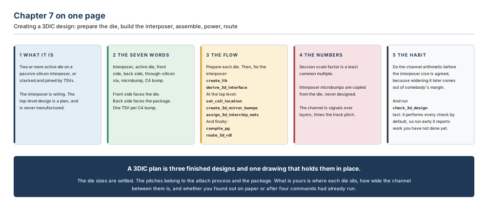
Where the next chapter goes, and why
The system is planned. Two active die have boundaries, bump fields and a pitch they agree on. An interposer created from an empty netlist carries 505 microbumps on its front side, 164 C4 bumps and 164 through-silicon vias on its back, a power mesh under each die and routes between them. A top-level design that will never be manufactured holds all three at coordinates and z levels, and ten check categories say the assembly is consistent.
What has been assumed throughout is that each die is one design — a thing with a boundary that somebody hands you. Chapter 8 stops assuming that. It is about managing design blocks: partitioning a design and committing a logical hierarchy cell to a physical hierarchy block early in the flow, and then creating multiple optimised abstract views for those blocks, containing only the information needed for placement, timing and other tasks. Its flow is four steps — explore the design hierarchy, create module boundaries with explore_logic_hierarchy, commit the blocks with commit_block, and create the placement abstracts with create_abstract.
The link back to this chapter is the same idea at a smaller scale, and it is worth holding on to. An active die in this chapter was a boundary plus an interface, with its contents invisible and irrelevant to the system that mounted it. A committed block in Chapter 8 is a boundary plus an interface too, with an abstract view that deliberately contains only what the level above needs. One is a piece of silicon and the other is a piece of a netlist, and both exist so that the thing above them can be planned without knowing what is inside.