CHAPTER SIX
Planning I/Os and Flip-Chip Bumps: Filling the Strip the Floorplan Left Empty
By the end of this chapter you will be able to check that a library is fit for a flip-chip design before you run a single command; to build an I/O ring and know where the ordering on each side begins; to work out how many pad cells a side will hold and how much room to leave over; to say how often a power pad must appear and in what order the signal pads must sit; to lay out a bump field in the three documented patterns and count the bumps each one produces; to pair pads with bumps automatically or by hand and say which you would defend; to insert the corner, break and filler cells that nobody asks for and everybody needs; to route, optimise and shield the redistribution layer; and to run the two different checks — one before placement and one after — that between them catch the mistakes this chapter can make.
Why this chapter matters in a real project
Chapter 4 drew a boundary and reserved a strip of silicon 120 µm deep all the way round it, and then left that strip completely empty. This is the chapter that fills it. Everything that connects the design to the outside world lives in there or just above it: the driver cells that shift signals on and off the die, the power and ground pads that feed the whole chip, the corner cells, the filler, and — for a flip-chip design — the field of bumps that the package will actually solder to.
What makes it worth reading slowly is not difficulty. Almost every step is arithmetic you could do on paper, and this chapter does exactly that, twice, for every number it uses. What makes it worth reading slowly is that the arithmetic runs into two constraints you did not set and cannot change. The pad cell's width and height come from the library. The bump pitch, and often the bump positions themselves, come from the package — and the package is frequently signed off before your floorplan is. So this is not a chapter about deciding how big things are. It is a chapter about fitting what you were given into the space you have, discovering early that it does not fit, and saying so while there is still time to move something.
The other reason for care is that the failures here are quiet in a particular way. A wrong design_type in the library is not reported by any command in this chapter; it simply means bump assignment does not happen for that cell, and the cell sits there looking placed. A guide created on the wrong side puts its pads facing into the die. A filler run that leaves a two-micron gap is an error you can read, but a filler run that leaves no gap on a ring with no slack in it was a ring you should never have built. None of these is subtle once you know to look, and the whole of Section 6.6 is about knowing where to look.
Prerequisites
Chapter 4 above all: the die, the core, and the core offset that this chapter fills — including the fact that the offset defaults to the minimum I/O cell height, which is the first hint that the library was always going to have a say. Chapter 2: units, and the habit of reading a value back rather than trusting what you typed. Chapter 3: routing rules and application options. Chapter 5: matching types are new here, but the discipline is the one Chapter 5 taught — a number you type is a decision nothing downstream will question.
How to read the numbers and the notation in this chapter
Every length in this chapter is in microns, because microns are what the I/O and bump commands are typed in. That is a change from Chapter 4, which worked in millimetres, and it is the single most common source of confusion in the whole flow — so here is the notation, spelled out, before anything else.
| You will see | Read it as | What you need to know |
|---|---|---|
| µm | microns, or micrometres | A length, one thousandth of a millimetre. Every command in this chapter is typed in these. Nimbus-8's die is 3,440 µm on each side, which is the same length as Chapter 4's 3.44 mm. 1 mm = 1,000 µm. |
| mm | millimetres | Used only when quoting a figure Chapter 4 fixed, and always with the micron value beside it, so you never have to convert while reading. |
| µm² | square microns | An area. It appears rarely here — this chapter is mostly lengths — and when it does, it is the same unit Chapter 5 used for a black box area. |
| × ÷ − | multiply, divide, subtract | Ordinary arithmetic with the proper signs, so a multiplication is never mistaken for the letter x and a subtraction is never mistaken for the hyphen that starts an option name. |
| 3,220 | three thousand two hundred and twenty | Commas group digits in threes so a long number reads at a glance. They are punctuation only: typed into a command the same number has no commas, 3220. |
| a square 3,440 µm on each side | a square whose sides are each 3,440 µm long | A shape and a length, not an area. Its area is a separate number, and this chapter always says which of the two it means. |
| Section 6.4.3 | section 6.4.3 of this chapter | A cross-reference. The first digit is the chapter, so anything beginning “6.” is in these pages. Follow it if you want the detail now; ignore it if you would rather keep reading. |
create_io_ring | a command, exactly as typed | Anything in this typewriter face is something you type, or a name the tool uses. Reproduced character for character: spelling and underscores matter. |
| -side | an option belonging to a command | The leading hyphen marks it as an option, not a subtraction. Options follow the command name, in any order, each with its value where it takes one. |
| {{6 VDD_EW} {6 VSS_EW}} | a nested Tcl list | Curly braces group things. The outer braces hold the whole list; each inner pair holds one item, here a number and the reference cell it applies to. Several options in this chapter take lists shaped exactly like this. |
The row to hold on to is the first one. Chapter 4 said the die is 3.44 mm and the core offset 0.12 mm; this chapter says 3,440 µm and 120 µm, and they are the same two lengths. Nothing about the design changed — only the unit the commands expect. When you see a bare number in an I/O or bump command with no unit attached, it is microns, and the first thing to do with any figure somebody hands you is ask which of the two units it is in.
Learning objectives
- Name the four kinds of flip-chip cell and the
design_typevalue each one must carry, and say which additional attribute a bump cell's pin and a driver cell's terminal each need. - Create an I/O ring or four I/O guides, and state where the pad ordering begins on each of the four sides.
- Compute how many pad cells a side will hold from the die size, the corner height and the pad width, and justify the slack you leave over.
- Write power and signal I/O placement constraints, and predict the pad sequence a given constraint file produces.
- Create a bump array in each of the three documented patterns and compute how many bumps each produces on the same grid.
- Assign pads to bumps both automatically and with matching types, and explain what
-uniquifyand the two special matching types do. - Insert corner, break and filler cells, and work out the filler cells a given gap requires under the largest-first rule.
- Route, optimise and shield RDL nets, and quantify what the routing-angle option is worth in wire length.
- Run
check_pre_place_ioandcheck_io_placement, say which belongs before placement and which after, and name at least six of the nine checks.
6.1 The beginner's mental model
Start with a terraced street
Picture a row of houses along one side of a street. They sit in a line, shoulder to shoulder, and what matters about any one of them is not its coordinates but its position in the row: third from the corner, next door to the substation. Where the row meets the next street there is a building on the corner that belongs to neither row.
Now look at the road itself. Set into it is a grid of service covers at a fixed spacing — not a spacing anybody on this street chose, but one the water company settled years ago. Every house needs a pipe from its own front wall down to one of those covers, and which cover it gets is a decision somebody has to make, house by house.
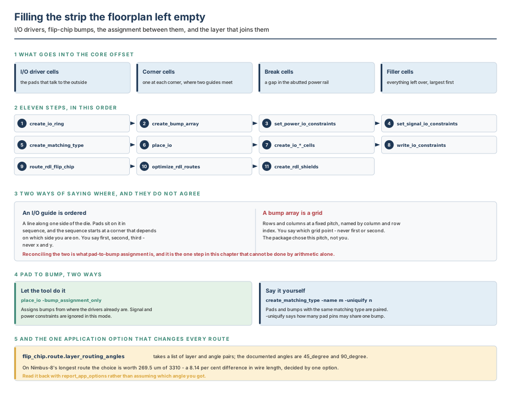
That is the whole chapter. The row of houses is an I/O guide: an ordered line of pad cells along one side of the die. The substation every few houses is a power pad, inserted at a ratio you specify. The corner building is a corner cell. The grid of covers is a bump array. The pipes are RDL routes. And the decision about which cover serves which house is pad-to-bump assignment, which is what matching types are for.
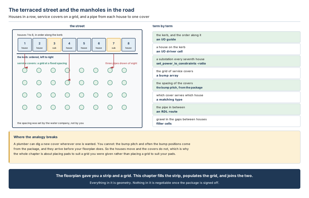
A plumber who finds no cover conveniently placed can dig a new one. You cannot. The bump pitch is a manufacturing and packaging constraint, and on most projects the bump positions themselves arrive as a file — which is exactly why read_aif exists and why Section 6.2.6 is about reading locations rather than choosing them. The houses can be re-ordered along the kerb all day. The covers do not move.
The second difference is about who finds out. If a pipe cannot reach its cover, the plumber notices on the day. Here the two halves of the problem are done by different commands at different times: you place pads, you create bumps, and only when place_io runs does anything try to pair them up. A pad count and a bump count that do not reconcile is not an error at either of the steps that produced them.
Now the engineering model
After the floorplan exists, you can instantiate the I/O drivers and the bump cells. The tool supports unconstrained and constraint-based placement of both, and it supports placement constraints that specify the ordering, the x-y coordinate and the placement side for each I/O. Both package-driven and die-driven flows are supported, and different driver styles — including pads with integrated drivers — are handled.
Two facts bound everything that follows. The first: chip I/Os can be placed along the chip periphery or in islands within the chip core. The periphery is the common case and the one this chapter builds, but nothing requires it. The second: the constraints come in exactly two kinds — signal constraints, which specify I/O adjacency requirements, and power constraints, which specify power requirements. Section 6.4.2 and Section 6.4.3 take one each, and the division between them is worth learning now because the two commands are easy to confuse.
The order of the work is fixed, and Figure 6.1's second panel gives it in full: rings or guides, then bump arrays, then power constraints, then signal constraints, then matching types, then place_io, then the physical-only cells, then the constraints written back out, then RDL routing, optimisation and shielding. Eleven steps. Only two of them — place_io and the RDL router — do anything you could call automatic; the other nine are you telling the tool what you have decided.
place_io runs.Do not confuse these
| This | Not this | How to tell them apart in one question |
|---|---|---|
| An I/O ring | An I/O guide | How many sides? A guide is one line along one side; a ring is a set of related guides, normally four. create_io_ring makes four guides and names them after the ring; create_io_guide makes one. |
| A bump cell | An I/O driver cell | Which one does the package touch? The bump is the connection to the package and carries design_type flip_chip_pad. The driver is the logic that shifts the signal and carries flip_chip_driver or pad. |
| A filler cell | A break cell | Does it complete the power rail or interrupt it? Filler completes the abutted power connection; break creates a space in it so two I/O voltages can meet. Both carry design_type pad_spacer. |
set_power_io_constraints | set_signal_io_constraints | Are you saying how often or in what order? Power constraints are about frequency, spacing and sharing; signal constraints are about sequence and gaps between named pads. |
check_pre_place_io | check_io_placement | Before or after? The first validates matching types, guides and the pad assignment file before place_io runs; the second validates the placement that came out. |
-ratio | -spacing | Counted in pads or in microns? -ratio is how many signal pads may sit between two power pads; -spacing is the maximum distance in microns between them. |
-share | -uniquify | Which object is being shared? -share on a power constraint says how many power pads may drive one bump. -uniquify on a matching type says how many pad pins may be assigned to one bump cell. |
create_bump_array | create_bump_pattern | Is there a region or a set of pads? The array fills a bounding box or boundary at a pitch. The pattern reads a file and places bumps in rows or columns relative to named I/O pad cells — for designs where pads are not placed using guides. |
| The bump pitch | The pad pitch | Who chose it? The bump pitch comes from the package and is given to create_bump_array -delta. A pad pitch is something you may impose with create_io_guide -min_pitch or a signal constraint. |
| Side-wall shielding | Coaxial shielding | Same layer or above and below? Side-wall shields on the same layer as the net. Coaxial shields above and below, gives better isolation, and uses more routing resource. |
6.2 The concepts, from first principles
6.2.1 The library, before anything else
Before beginning a flip-chip design you must ensure that the reference library containing the flip-chip component cells is properly configured. That sentence is easy to skim past, and it is the most expensive sentence in the chapter to ignore, because the configuration in question is a single attribute on each of four kinds of cell and nothing later reports a wrong one.
The attribute is design_type, and the four values are these. Bump cells must have it set to flip_chip_pad. Driver cells must have it set to flip_chip_driver or pad — or to macro, if the flip-chip matching types are defined. Filler and break cells must have it set to pad_spacer, one value covering both. Corner cells must have it set to corner.
Two of those four need something more than design_type. On the library cell pin of a bump cell, the is_pad attribute must be set to true — and the reason is specific: you must set this attribute for the tool to automatically create terminals for top-level ports when bumps are connected or assigned to ports. On a driver cell, the terminal or pin shape that will be connected to an RDL route should have the class attribute set to bump; if there is no terminal with that setting, the RDL router chooses the topmost layer terminal of the port instead. That is not an error. It is a different route from the one you intended, chosen silently.
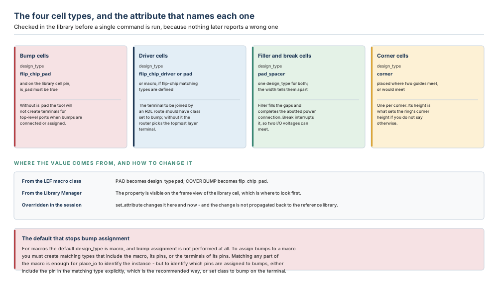
Where does the value come from? Often from the LEF file for the library cell, and the mapping is worth knowing because it explains most of what you will find already correct: a value of pad is created from the PAD macro class, and a value of flip_chip_pad from the COVER BUMP macro class. Property types and attribute settings on the frame view can be examined in the Library Manager, which is the first place to look. And some attributes of a library reference cell can be overridden with set_attribute in the tool — with one consequence stated plainly in the reference and worth repeating: attribute settings performed in the tool are not propagated to the reference library. Your override lives in this session and dies with it unless the script that set it is kept.
Because for macros the default design_type is macro, and with that value bump assignment is not performed. Not badly performed — not performed. The macro is not considered an I/O cell, so no bumps are assigned to its RDL pins, and the tool has no reason to tell you so.
The fix is to create matching types that include the macro, its pins, or the terminals of its pins. Matching any part of the macro is sufficient for place_io to identify the cell instance. But identifying the instance is not the same as identifying which pins get bumps, and for that you have two choices: include the pin in the matching type explicitly, which the reference recommends, or set class to bump on the terminal during library preparation or with set_attribute. Section 6.4.4 comes back to this with the exact commands.
design_type values, plus is_pad on a bump cell's pin and class equal to bump on a driver's RDL terminal. Check all six in the library before the first command, because none of them is reported wrong afterwards — they are reported as work not done.6.2.2 Rings, guides, and which end is the beginning
An I/O guide forms a placement area for I/O drivers. You can create an I/O ring by placing four guides along the periphery with four create_io_guide commands, or by using one create_io_ring command. Multiple rings are supported, and so are multiple guides on the same side of the die.
The ring is the convenient form, and it names its guides for you:
icc2_shell> create_io_ring -name outer_ring -corner_height 300
{outer_ring}
icc2_shell> get_io_guides
{outer_ring.left outer_ring.bottom outer_ring.right outer_ring.top}
Four guides, named by adding .left, .top, .right and .bottom to the ring name. If you do not name the ring it is called _default_io_ring followed by an index, which is why that name turns up in so many examples.
The four-command form gives you control of the exact geometry, and it is where the one genuinely confusing option lives:
icc2_shell> create_io_guide -name "ring_left" -line {{0 300} 3000} -side left
{ring_left}
icc2_shell> create_io_guide -name "ring_top" -line {{300 3640} 3000} -side top
{ring_top}
-line takes a starting point and a length, and it is required. -side is also required, and it does more than label the guide: it indicates the orientation by specifying the outer edge. Left and right lines must be vertical; top and bottom lines must be horizontal. And the pads of a left guide are aligned on the right side of the guide line — because the line is the outside of the die and the pads sit inward from it.
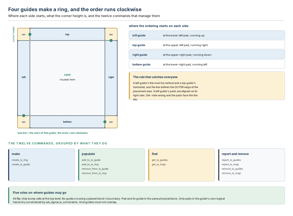
The clockwise rule is the thing to memorise, because every signal constraint you write depends on it. Signal ordering begins at the lower-left pad for the left edge, the upper-left pad for the top edge, the upper-right pad for the right edge, and the lower-right pad for the bottom edge. So the starting point of a left guide is the bottom end of its line, and the starting point of a right guide is the top point of its line. A constraint that lists three pads in order produces a different physical arrangement on the left side than on the right, and both are correct.
Guides may be placed anywhere in the hierarchy provided five rules are honoured, and they are worth reading as a checklist rather than as prose. All flip-chip bump cells must be placed at the top level. Guides are not allowed to cross block boundaries for a placed block. An I/O pad cell and its associated guide must be placed within the same physical block instance. Only pads in the same logical hierarchy as the guide can be constrained with set_signal_io_constraints. And guides must not overlap.
Twelve commands manage rings and guides, and they divide into four jobs. Two make them: create_io_ring and create_io_guide. Four populate them — add_to_io_guide adds pad cells to a guide, add_to_io_ring adds guides to a ring, and remove_from_io_guide and remove_from_io_ring undo each of those. Two find them: get_io_guides and get_io_rings return collections. And four report or remove them: report_io_guides and report_io_rings print them — both take -verbose and -significant_digits — while remove_io_guides and remove_io_rings delete them from the block. The four in the middle are the ones worth knowing early: a ring built with the wrong corner height is edited, not rebuilt, and editing it leaves every constraint that names a guide intact.
| Option | What it decides | Default if you say nothing |
|---|---|---|
| create_io_ring -name | The ring name, used as the prefix for its guides | _default_io_ring plus a positive integer |
| create_io_ring -corner_height | The distance between the ring's outer and inner bounding boxes | the height of the tallest pad cell assigned to the ring; failing that, the height of the shortest pad cell in the design |
| create_io_ring -bbox | The bounding box for the ring | the inner bounding box of the smallest existing ring, or the die area if there is no ring |
| create_io_ring -inside | An existing ring to use as the outer boundary for this one | none; used to build concentric rings |
| create_io_ring -offset | The distance from the target boundary to the new ring's outer boundary | 0 |
| create_io_ring -guides | Existing guides to group into a ring. Cannot be combined with anything but -name. | none; and a ring built this way keeps a corner height of 0 until you set it |
| create_io_ring -pad_cell_list | Pad instances to assign to the guides inside the ring; spread evenly if they fit | none; an empty ring is legal |
| create_io_guide -line | The guide's outer edge, as a start point and a length, in chip coordinates | required |
| create_io_guide -side | Which outer edge this is: left, right, bottom or top | required |
| create_io_guide -name | The guide name | default_guide plus a positive integer |
| create_io_guide -offset | The minimum gap from the guide's start to the first pad, and from the last pad to its end | both gaps are zero |
| create_io_guide -pad_cells | Pad cells to include. An error if a cell's reference is not a pad type, or is already on another guide. | none; an empty guide is legal |
| create_io_guide -min_pitch | A minimum pitch between drivers on this guide, honoured during place_io | none |
-min_pitch AND A CONSTRAINT DISAGREES WITH IT?
The constraint wins. If there are conflicts between the minimum pitch and the signal or power I/O constraints, the tool honours the signal and power constraints first. There is a second limitation worth knowing at the same time: if the design has multiple rings, the result is only guaranteed when there is no overlap between pads and I/O guides.
The practical reading is that -min_pitch is a floor you set once for a whole side, and a signal constraint is a specific instruction about named pads. When they disagree the specific instruction is taken to be the more deliberate of the two — which is almost always right, and is exactly the behaviour you would want if you had thought about it, but is not what most people assume when they set a minimum and expect it to be absolute.
-line gives the outer edge and -side says which edge it is; get the second wrong and the pads face inward.6.2.3 Nimbus-8's ring, and the arithmetic that fills it
Everything so far has been mechanism. Here is what it comes to on the design this book has been carrying.
Chapter 4 fixed Nimbus-8's die at a square 3,440 µm on each side and its core at a square 3,200 µm on each side, leaving a core offset — the strip this chapter fills — 120 µm deep on all four sides. The library offers pad cells 110 µm tall and 46 µm wide, and a corner cell that is a square 110 µm on each side. The 110 against the 120 is the first check to make and the easiest to forget: a pad taller than the offset does not fit in the strip at all, and 10 µm of margin is comfortable rather than generous.
The guide length follows from the die and the corner cells, because the corners belong to neither side:
3,440 − 2 × 110 = 3,220 µm of guide, on each of the four sidesHow many pads is that? At 46 µm each, 3,220 ÷ 46 = 70 exactly. It is tempting, and it is the wrong answer, and the reason is worth stating as a rule: a ring filled to its exact length has no slack, and a ring with no slack cannot be adjusted. Seventy pads leaves nothing for filler cells, nothing for break cells, and nothing for the spacing a power constraint may ask for. So Nimbus-8 fills 56 slots per side and keeps the difference:
56 × 46 = 2,576 µm of pad cell
3,220 − 2,576 = 644 µm of gap, which is 20.0 per cent of the guide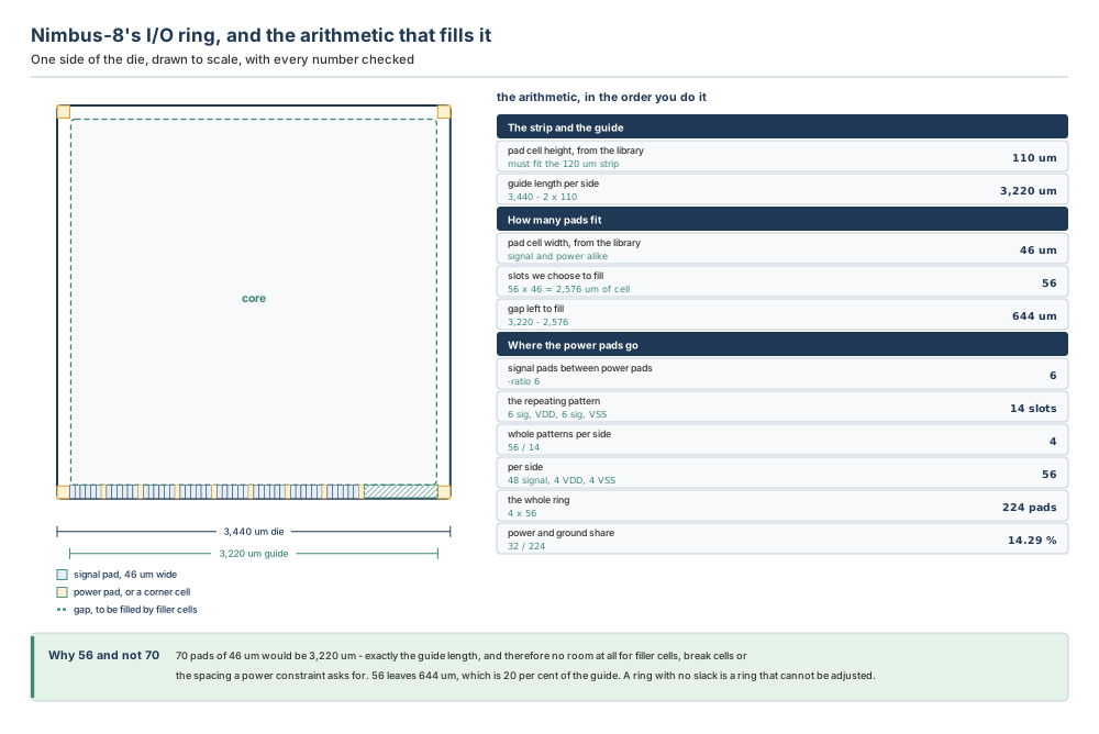
Now the power pads. Section 6.4.2 gives the command; what matters here is the arithmetic it implies. A ratio of 6 means no more than six signal pads between successive power pads of that type, and with a VDD constraint and a VSS constraint both at 6 the repeating unit is six signal pads, a VDD, six more signal pads and a VSS — fourteen slots holding twelve signal pads and two power pads. Fifty-six divides by fourteen exactly four times, so each side carries
4 × 12 = 48 signal pads,  4 VDD,  4 VSS  =  56 slots
and the whole ring:  4 × 56 = 224 pads  =  192 signal + 32 power
Power and ground are 32 of 224, which is 14.29 per cent of the ring. Check it the other way: 192 ÷ 224 = 85.71 per cent signal, and the two shares sum to 100.
The choice of 56 rather than 70 is the only judgement on this page, and it is the one an interviewer will ask about. Twenty per cent slack is a defensible number and not a magic one; some teams work to fifteen, some to twenty-five. What is not defensible is filling the ring exactly and discovering at the filler step that there is nowhere to put a break cell.
The other thing to notice is that 56 divides exactly by 14. That is not luck — it is the reason 56 was chosen over 55 or 58. When a ratio produces a repeating pattern, picking a pad count that is a whole number of patterns means every side comes out identical, and identical sides are far easier to review than four sides that each end differently.
6.2.4 Bump arrays, and the three patterns
The tool supports bump cell placement for flip-chip designs, and there are two routes to it. You can place bump cells from coordinates in a DEF or AIF file — Section 6.2.6 — or you can create a bump array with create_bump_array, which is the die-driven flow: you create a region for bump placement and let the tool determine the locations. One sequencing rule governs both: you should place bump cells before placing I/O driver cells.
create_bump_array has two required options and they are the two that matter most. -delta gives the horizontal spacing between adjacent columns and the vertical spacing between adjacent rows — the bump pitch, which came from the package. And one of -lib_cell or -lib_cell_collection names the bump library cell; all bump instances in an array must have the same library cell.
| Option | What it decides | Default if you say nothing |
|---|---|---|
| -delta {dx dy} | Horizontal spacing between columns and vertical spacing between rows | required |
| -lib_cell | The bump library cell, as a cell name, or library and cell, or library, cell and view | required, unless -lib_cell_collection is used |
| -lib_cell_collection | The same thing as a collection. If several cells are given, only the first is used. | mutually exclusive with -lib_cell; one of the two is required |
| -name | The array name, which also names the bumps: name, then column index, then row index | default_bump_array plus a positive integer |
| -bbox | A rectangular region to place within; no bump may extend beyond it | with neither -bbox nor -boundary, the entire design area |
| -boundary | A rectilinear region to place within. Mutually exclusive with -bbox. | as above |
| -exclude_regions | Regions of the boundary to leave empty | none |
| -pattern | inline, staggered_1 or staggered_2 | inline |
| -repeat {columns rows} | The total number of columns and rows. No bumps are created outside the bounding box even if you ask for more. | the command fills the bounding box or design area |
| -origin {x y} | The spacing from the array bounding box's lower-left corner to the lower-left corner of the bump at column 0, row 0 | with -repeat given, derived so the array is centred; otherwise (0,0) |
| -origin_spec bl | c | Whether -origin means the lower-left corner or the centre of that first bump | — |
| -orientation | The orientation of every bump: N, W, S, E, FN, FS, FE or FW | N |
| -non_overlap | Place only bumps that do not overlap existing ones | not specified |
| -ring_depth {count} | The width and height of the ring | not specified |
| -allow_block | Allow a block as the reference cell | not specified |
The three patterns are the part worth drawing, because the names do not tell you how many bumps you get. inline places a bump at every point in the array defined by -delta. staggered_1 places bumps only where the sum of the column index and the row index is even. staggered_2 places them only where that sum is odd. On any grid, the two staggered patterns are complements of one another and each gives you about half as many bumps as inline — exactly half when the number of grid points is even, and one more or one fewer when it is odd.
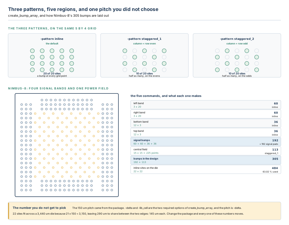
Nimbus-8's bump field is five arrays, following the shape of the framework's own example: four peripheral bands for signal, and one central field for power and ground. The pitch is 150 µm, which came from the package. Twenty-two sites fit across the die, because twenty-one gaps of 150 µm span 3,150 µm and the remaining 290 µm splits into 145 µm at each edge.
The four signal bands are 3 columns × 20 rows on the left and right and 12 columns × 3 rows on the top and bottom, which gives
2 × (3 × 20) + 2 × (12 × 3) = 120 + 72 = 192 signal bumpsand 192 is exactly the number of signal pads the ring holds. That agreement is the point of the whole section, and it did not happen by itself — the band depths were chosen to produce it.
The central field is a 15 × 15 grid at the same pitch with -pattern staggered_1. Of its 225 points, the ones with an even column-plus-row sum number
8 × 8 + 7 × 7 = 64 + 49 = 113 bumpsbecause there are 8 even indices and 7 odd ones in 0 to 14, and an even sum needs both indices even or both odd. Total: 192 + 113 = 305 bumps, against 484 sites if the whole die were filled inline — 63.02 per cent of them used.
“staggered_1 halves the bump count, so it halves the current the field can carry.”
It halves the count, and that much is arithmetic. What it buys is the reason to use it: a staggered field leaves a clear diagonal channel between every pair of bumps, which is where the RDL routes go. An inline power field at the same pitch has more bumps and less room to route to them, and on a design where the RDL is congested the staggered field with fewer, better-reachable bumps carries more current in practice than the dense one you cannot wire up.
That is a judgement, not a documented rule, and it is the kind of judgement to make with the RDL router's own report rather than from first principles. The documented facts are only these: which points each pattern keeps, and that inline is the default.
6.2.5 When the pads are not on guides: bump patterns from a file
Everything above assumes an I/O ring. In designs where the pad cells are not placed using guides — clusters of I/O cells in the core, area-array pads, an island — create_bump_pattern instantiates bump cells relative to named pads instead of relative to the die. It is the right tool when the requirement is that bump cells sit in rows or columns perpendicular to the I/O pad cells.
The command takes a file, and the file is where all the work is:
icc2_shell> create_bump_pattern -file_name bump_patterns.txt
12 bumps and 5 matching types are created successfully
Two things about that response are worth pausing on. It reports bumps and matching types — the pattern file creates both, so this one command does a job that would otherwise be create_bump_array plus several create_matching_type calls. And the matching types it creates are named from the matching-type prefix in the file plus the first I/O pad named, which is why the framework's own example produces names like g0_bus_3 from a prefix g0_ and a first pad bus_3.
The file's format is documented in full and is more than this chapter needs to teach in detail, but its shape is worth knowing: a bump_lib_cell line naming the bump cell, a bump_pitch line in microns, and one or more io_group blocks. Each group lists the I/O pad instance names, each in its own braces with an optional matching-type prefix — and if no prefix is given, the prefix s is used. Each group may also state an orientation of row, column or perpendicular, and then one or more ordering-and-spacing sections giving a centre-line offset, a first-bump spacing on the left or bottom, the matching-type prefixes for that side, a first-bump spacing on the right or top, and the prefixes for that side. Comments begin with a hash for a whole line or two forward slashes inline.
orientation KEYWORD OUT?
The command decides for you, from the shape of the I/O pad bounding box. If the width is greater than the height, the bump cells are placed in columns. If the height is greater than the width, they are placed in rows.
That is a sensible default and a poor thing to rely on, because the shape of a pad cluster's bounding box can change when somebody adds a pad. State the orientation.
6.2.6 When the package has already decided: reading locations
If the locations of the bump cells are determined by the constraints of the package — which on a production design they usually are — you do not create an array at all. You read the positions in with read_aif:
icc2_shell> read_aif bumps.aifThe location information is typically held in a DEF or an AIF file containing x- and y-coordinates and bump cell names for the bumps in the block. An AIF file's [DIE] section gives a width and a height, its [PADS] section defines the bump cell outlines, and its [NETLIST] section lists one line per bump with a net name, a pad type and a pair of coordinates. The coordinates in the framework's example are negative as well as positive, which is the first clue that the file's origin is the die centre rather than a corner — a detail to check against your own file rather than to assume.
One option deserves naming: -hierarchy reads in bump cell and I/O pad locations and places the I/O pads in any level of physical hierarchy. On a flat design you will not need it. On the multi-level design of Section 6.2.7 it is the difference between a file that works and one that places everything at the top.
create_bump_array when you choose the positions, create_bump_pattern when the positions follow named pads, and read_aif when the package has already chosen. On a production flip-chip design the third is the common case.6.2.7 More than one level of hierarchy
The tool supports top-level and block-level flip-chip planning for designs with multiple levels of physical hierarchy, and the governing behaviour is a single sentence: performing top-level flip-chip routing connects bump cells at the top level and ignores bump cells within the blocks. Everything else follows from that.
Seven considerations apply, and they read as a set of constraints on how the design must be organised. Blocks which contain I/O bump cells or pad cells must be preplaced. I/O pad cells may be at the top level or the block level, and those at the block level are considered fixed. I/O guides are created at the top level. Matching types that assign top-level bumps to block-level I/O cells must be created at the top level. I/O pads are placed at the block level for blocks that contain them. Block-level I/O pads should be specified with create_matching_type. And for block-level pads not specified that way, the pin shapes should have their class attribute set to bump in the Library Manager.
That last pair is the same choice Section 6.2.1 offered for macros, appearing again in a different place: name the object in a matching type, or mark its terminal in the library. Naming it is more work and more explicit, and the reference recommends it both times.
There is also a documented frame-based flow for tool versions before N-2017.09, which prepares the frame view of a block for I/O assignment by pushing into the block with set_working_design -push, optionally creating terminal shapes for power and ground pins with create_shape -port, running create_frame, popping back out, changing the block's view with change_view -view frame, setting its design_type to flip_chip_driver and setting the terminals' class to bump.
If you are on a current release you will not need it. It is in this chapter for one reason: if you inherit a script that does all of that, it is not wrong, it is old, and knowing which of the two you are looking at saves an afternoon. The note about run_block_script in the same passage is worth keeping either way — creating frame views for many blocks is faster from a script run that way than one block at a time.
6.3 Inputs, outputs and readiness
This chapter needs more from outside the tool than any chapter so far: a library that has been checked, and a package that has been decided. Both are other people's work, and both arrive on their own schedule.
| Stage | What you need | Why |
|---|---|---|
| Before the first command | A floorplan with a core offset deep enough for the pad cells | The strip is where the ring goes. A pad taller than the offset does not fit, and the offset defaults to the minimum I/O cell height precisely because of this. |
| The reference library, with all six attributes checked | Section 6.2.1. Four design_type values, is_pad on a bump pin, class equal to bump on a driver terminal. | |
| The pad cell height and width, and the corner cell size | Guide length and pad count are computed from these, not chosen. | |
| The bump pitch, and the bump positions if the package has fixed them | -delta is a required option of create_bump_array, and on a production design the positions arrive in a DEF or AIF file. | |
Before place_io | Bump cells placed | Stated as a rule: place bump cells before placing I/O driver cells. |
| Power and signal constraints set, or a deliberate decision not to | With no power constraints, place_io spreads the power pads evenly through the guide. That is a default, not an absence of a decision. | |
Matching types created, and check_pre_place_io run clean | Six consistency checks that are much cheaper before placement than after. | |
| Before RDL routing | A routing rule with widths and spacings, and shield widths if you will shield | The shield options belong on the rule, set when the rule is created, not later. |
| The routing rule applied to the RDL nets | set_routing_rule on the nets of the flip-chip pads' pins. | |
| The routing angle decided for each layer | Worth 8.14 per cent of wire length on Nimbus-8's longest route. Section 6.4.6. | |
| Afterwards you have | A populated strip, a bump field, and every pad paired with a bump | Nine checks confirm it, and write_io_constraints records it so the next run reproduces it. |
| RDL routes, optionally optimised and shielded | And a report that names any open net. |
Preflight checklist
- The library has been checked: bumps
flip_chip_padwithis_padtrue on the pin; driversflip_chip_driver,padormacrowithclassequal tobumpon the RDL terminal; filler and breakpad_spacer; cornerscorner. - The pad cell height is less than the core offset. Write both numbers down side by side.
- Guide length computed as the die side less two corner heights, and pad count computed from it — with slack left over deliberately, and the percentage recorded.
- The bump pitch is the package's number, read from the package document rather than inferred from a drawing.
- You know whether bump positions are yours to choose. If they are not, you are using
read_aifand notcreate_bump_array. - The signal pad count and the signal bump count have been compared, and they agree — or you know by how much they do not and what you intend to do about it.
- Every length you are about to type is in microns.
check_pre_place_iohas been run and is clean, beforeplace_io.
Item 6 is the one that is never on anybody's checklist and should be. Two counts produced by two different commands at two different times have to be equal, and nothing compares them until place_io tries to pair them up. Compare them yourself, on paper, before you run anything: signal pads on one line, signal bumps on the next, and the difference on the third. On Nimbus-8 both are 192 and the difference is zero, which took two attempts at the band depths to achieve.
6.4 The guided tool walkthrough
6.4.1 create_io_ring and create_io_guide — the placement area
Purpose. Create or group a related set of I/O guides used for I/O placement; or create one line-based I/O pad constraint for I/O placement. Guides must exist before I/O cells are placed.
Syntax in plain English. The ring form takes a name and a size and makes four guides. The guide form takes a line, a side, and optionally a name, offsets, pad cells and a minimum pitch. Table 6.3 has every option; the examples below are the four shapes you will actually type.
# The whole ring in one command, with the corner height stated.
icc2_shell> create_io_ring -name nimbus_ring -corner_height 110
icc2_shell> get_io_guides
{nimbus_ring.left nimbus_ring.bottom nimbus_ring.right nimbus_ring.top}

# Or four guides, when you want the geometry exactly.
icc2_shell> create_io_guide -name ring_left -line {{0 110} 3220} \
   -side left -offset {0 0}
icc2_shell> create_io_guide -name ring_top -line {{110 3440} 3220} \
   -side top -offset {0 0}

# A second ring inside the first, 200 um in.
icc2_shell> create_io_ring -name inner_ring -inside nimbus_ring \
   -offset 200

# A ring made by grouping guides that already exist.
icc2_shell> create_io_ring -name grouped -guides [get_io_guides]
Expected result. A ring holding four guides named after it, or one guide. An empty ring or guide is legal; pads can be added later.
Verification. get_io_guides and get_io_rings return collections, and report_io_guides and report_io_rings print them — both take -verbose and -significant_digits. Read the guide back and check its length against your arithmetic, because a -line length you typed is not a length the tool computed.
Common mistakes. Getting -side wrong, so the pads sit on the wrong side of the line and face into the die. Building a ring with -guides and then wondering why its corner height is zero — that form leaves it at zero until you set it. Assuming the ordering starts at the same corner on every side. Letting two guides overlap. And relying on the default corner height, which is the tallest pad assigned to the ring, on a ring that has no pads assigned yet.
Prerequisites. A floorplan, so that the die area exists to place the ring in.
Finding the rest. man create_io_ring and man create_io_guide; the Floorplan Task Assistant also builds both, under Floorplan Preparation, I/O Planning, I/O Ring and Guide.
6.4.2 set_power_io_constraints — how often the power pads appear
Purpose. Specify spacing and other requirements for power I/O drivers, so that place_io places them into the guides accordingly.
Syntax in plain English. Either a positional constraint description in braces, or four options that each take a list of value-and-reference-cell pairs. The two forms do the same job; the option form is easier to read and easier to diff.
# The positional form, as the framework writes it: a reference cell,
# a ratio, a name prefix, and the pin-to-net connections.
icc2_shell> set_power_io_constraints \
   -io_guide_object [get_io_guides "*left *right"] \
   {{reference: VDD_EW}
    {ratio: 6}
    {prefix: VDD}
    {connect: {VDDIO VDDIO} {VDD VDD1} {VSS VSS1}}}
# The option form, for two reference cells at once.
icc2_shell> set_power_io_constraints \
   -reference_cell {VDD_EW VSS_EW} \
   -ratio {{6 VDD_EW} {6 VSS_EW}}

# A maximum distance instead of a count, and a first-pad offset.
icc2_shell> set_power_io_constraints -reference_cell {VDD_NS VSS_NS} \
   -spacing {{100 VDD_NS} {100 VSS_NS}} \
   -offset {{100 VDD_NS} {100 VSS_NS}}

# Two VDD pads may drive one bump; three VSS pads may drive one.
icc2_shell> set_power_io_constraints \
   -reference_cell {VDD_NS VSS_NS} -share {{2 VDD_NS} {3 VSS_NS}}
| Option | What it decides | Counted in |
|---|---|---|
| -ratio | How many signal pads may be placed between successive power pads of that type | pads |
| -spacing | The maximum spacing between successive power pads of the same type | microns |
| -offset | The maximum distance from the guide's starting point to the closest edge of the first power pad of that type | microns |
| -share | How many power pads may be assigned to drive a single bump cell | pads per bump |
| -reference_cell | Which power pad cell references the constraint applies to | — |
| -io_guide_object | Which guides it applies to; patterns work, so "*left *right" catches two sides of every ring | — |
Expected result. The constraint is recorded and reported set. Nothing moves until place_io runs.
Verification. The only real verification is after placement: check_io_placement -power_constraints. Before that, re-read the constraint you typed and check the arithmetic implies the pad count you expect — on Nimbus-8, a ratio of 6 on both cells means a repeating unit of 14 slots, and 56 divides by 14 exactly four times.
Common mistakes. Confusing -ratio with -spacing — one counts pads, the other counts microns. Setting a ratio whose repeating unit does not divide the pad count, so the four sides end differently. Forgetting -io_guide_object, so a constraint meant for two sides applies to all four. And assuming that setting no constraint means no behaviour: with none set, place_io places the power pads evenly throughout the guide.
Prerequisites. The guides must exist. The power pad cell references must be in the library.
Finding the rest. man set_power_io_constraints.
6.4.3 set_signal_io_constraints — in what order, and how far apart
Purpose. Specify the ordering and spacing for signal I/O drivers, for guides at the top level or within lower levels of the hierarchy.
Syntax in plain English. One of four sources: a constraint given inline, a constraint file, a CSV file, or a CSV file plus a map file that translates your column names into the ones the tool knows.
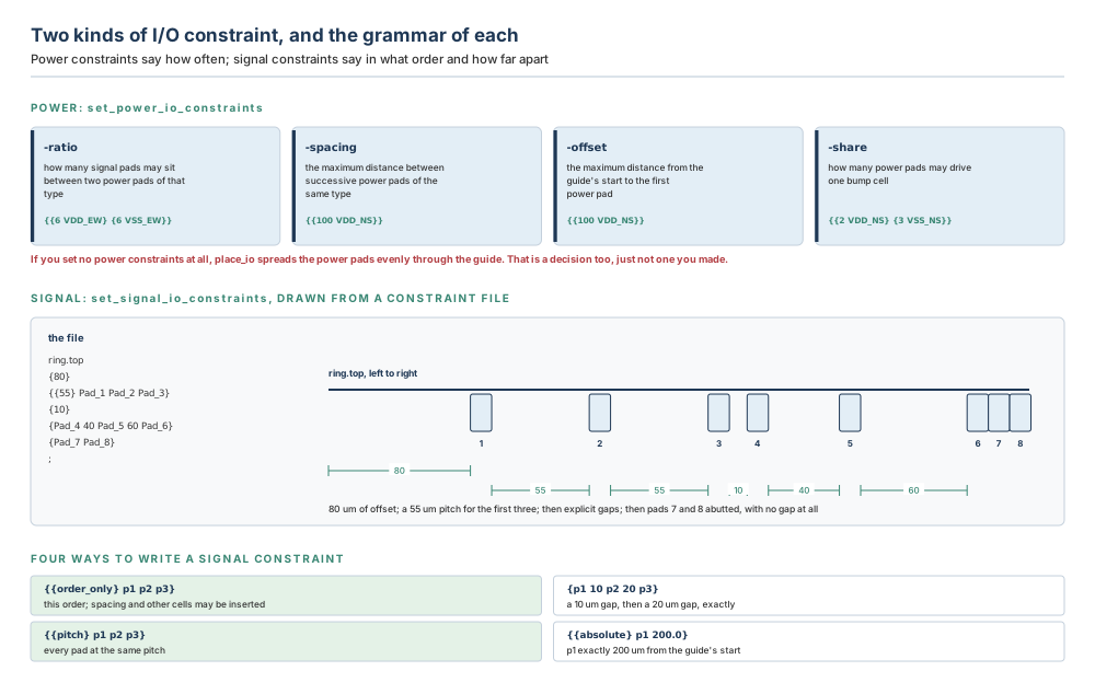
# Order only, inline. Spacing and other cells may still be inserted.
icc2_shell> set_signal_io_constraints -constraint {{order_only} \
   u_p/clk_pad_P1 u_p/sdclk_pad_P1 u_p/test_so_4_pad_P1} \
   -io_guide_object {_default_io_ring1.left}

# The same thing from a file, which is what you use in earnest.
icc2_shell> set_signal_io_constraints -file signal_io_constraints.txt

# From a CSV file, which only needs a "Pad Name" column.
icc2_shell> set_signal_io_constraints -csv iopads.csv \
   -io_guide_object io_guide_1

# From a CSV with your own column names, plus a map file.
icc2_shell> set_signal_io_constraints -csv ioconstraints2.csv \
   -io_guide _default_io_ring1.left -map_file map.txt
| Written as | Means | What it does not fix |
|---|---|---|
| {{order_only} p1 p2 p3} | Place these pads in this order | The gaps. Additional spacing and other pad cells might be inserted between adjacent pads. |
| {p1 10 p2 20 p3} | A 10 µm space between p1 and p2, and 20 µm between p2 and p3 | Where the group starts, unless an offset is given too. |
| {{pitch} p1 p2 p3} | Place each of these at the given pitch | Nothing within the group; the pitch is the whole specification. |
| {{absolute} p1 200.0} | p1 exactly 200 µm from the guide's start | The order of anything else, which needs its own constraint. |
| {80} | A bare number is an offset at that point in the file | — |
The CSV rules, because they are strict. The file must contain a header row defining the field order. Only the “Pad Name” field is required; “Offset Value” is optional. Any other fields are read and ignored — so a “Comment” or a “ref_cell” column is harmless. Fields may appear in any order, must not be repeated, and the number of fields must be the same in every row. If your columns have custom names, a map file of comma-separated pairs translates them, and the tool echoes each translation as it reads it.
By default place_io places I/O pads into the guides and overlaps any existing fixed objects. If something is already sitting at the start of a guide — a pad somebody placed by hand, a block edge — the placer will put pads on top of it.
The documented remedy is a constraint file containing both an absolute constraint and an order-based constraint, with the same pad named in both. The absolute constraint holds the first pad away from the object; the order-based constraint then sequences everything after it. Naming the same pad twice looks like a mistake and is not: it is what ties the two constraints together.
Expected result. “Signal IO constraints set successfully”. Again, nothing moves until place_io runs.
Verification. check_io_placement -signal_constraints after placement, which checks order, pitch, spacing, offset of pads and boundary spacing. And write_io_constraints, which writes the constraints implied by the current placement — so writing them out and diffing against what you set is a direct check that the placer did what you asked.
Common mistakes. Forgetting that the ordering starts at a different corner on each side. Using order_only and then being surprised that gaps appeared. Repeating a field in a CSV file, or giving rows with different field counts. And expecting an absolute constraint to imply an order.
Prerequisites. The guides must exist, and only pads in the same logical hierarchy as the guide can be constrained.
Finding the rest. man set_signal_io_constraints and man write_io_constraints.
6.4.4 create_matching_type and place_io — pairing, then placing
Before routing flip-chip drivers to bump cells you must create assignments between them, and there are two ways.
Automatic. place_io -bump_assignment_only does only bump assignment: no pad placement, and I/O driver cells are not moved. It assigns bumps to drivers based on their current locations — and it is important to know what it ignores: all the signal I/O constraints and power I/O constraints are ignored in this mode. It also does not work with -pad_assignment_file, and it is mutually exclusive with -skip_bump_assignment.
User-specified. A matching type has two jobs: it provides driver-to-bump pairing, and it provides support for driver placement. The tool assigns flip-chip drivers to bump cells that have the same matching type.
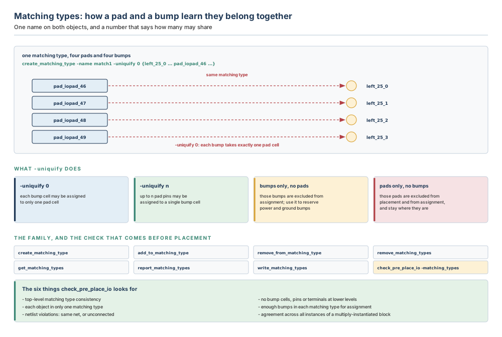
# Four pads to four bumps, one pad per bump.
icc2_shell> create_matching_type -name match1 -uniquify 0 \
   {left_25_0 left_25_1 left_25_2 left_25_3 \
    pad_iopad_46 pad_iopad_47 pad_iopad_48 pad_iopad_49}

# Check the matching types before placing anything.
icc2_shell> check_pre_place_io -matching_types
# Then place. This is the command that applies the assignments.
icc2_shell> place_io

# Find the cells that carry a given matching type.
icc2_shell> get_cells -filter "matching_type.name == SIGNAL"
icc2_shell> get_cells -filter "matching_type.name =~ SIG*"

# Write out what the tool assigned by itself, and read it back.
icc2_shell> write_matching_types -from_existing_assignment \
   -file_name existing.tcl
icc2_shell> source existing.tcl
Six more commands manage matching types once they exist, and they are the reason a hand-written assignment is maintainable rather than a one-off. get_matching_types returns a collection of them by name. add_to_matching_type adds pads or bumps to one that already exists, and remove_from_matching_type takes them out again. report_matching_types lists each type with its uniquify number, object type and object names, which is the form to paste into a review. remove_matching_types deletes named types, or all of them with -all. And write_matching_types writes your own definitions to a file, or with -from_existing_assignment writes out what the tool decided on its own — a file you can read, edit and source back, which is what makes “automatic first, then correct by hand” a workable habit rather than a compromise.
| Option | What it decides | Default if you say nothing |
|---|---|---|
| -io_guide | Place drivers only in these guides; drivers elsewhere are ignored and stay put | all guides, plus drivers not assigned to any guide |
| -matching_types | Place only the drivers named in these matching types | all existing matching types, plus drivers in none of them |
| -rule | A single routing spacing rule for pathlines; flip-chip designs only | a rule satisfying the rules set on all RDL nets; failing that, derived from the technology file |
| -pad_assignment_file | Which guides each named pad is allowed on. Lines of pads then guides, ending in a semicolon. | unassigned pads go to a guide the command chooses |
| -include_unassigned_pads | Assign and place unassigned or unconstrained drivers too | they are not placed, unless both -io_guide and -matching_types are omitted |
| -incremental | Place from each cell's spacing and offset attributes; non-flip-chip designs with no I/O constraints. Guide dimensions and bump distribution are not considered, and I/O constraints are ignored. | not specified |
| -skip_bump_assignment | Place pads only, no bump assignment. Excludes -bump_assignment_only. | both are done |
| -bump_assignment_only | Bump assignment only, from current driver locations. Signal and power constraints are ignored. Excludes -skip_bump_assignment. | both are done |
| -match_terminals_to_bumps | Match each terminal of a pin to a bump, for terminals labelled bump with no one-to-one logical connection to a bump already | not specified |
Because both are useful, and both are documented behaviours rather than side effects.
A matching type containing only bumps excludes those bumps from bump assignment; they are not connected to any pad pins unless they were already connected in the original netlist by two-pin nets. That is how you reserve bumps for power and ground and stop the assigner from wiring signals to them.
A matching type containing no bumps excludes its pads from I/O placement; they remain at their current position and are not processed during bump assignment. That is how you protect pads you have placed by hand.
And when a matching type contains both, place_io assigns bumps to pad pins according to the uniquify number, with any excess bumps or pad pins left unassigned. Excess is not an error either.
Verification. check_pre_place_io -matching_types before, and after placement the RDL Flylines panel in the GUI or — better for a script — write_matching_types -from_existing_assignment and read the file. report_matching_types prints a matching type with its uniquify number, object types and object names.
Common mistakes. Running -bump_assignment_only and expecting the signal constraints to be honoured. Forgetting that place_io removes existing filler cells unless their physical_status is fixed — which happens when all pads are considered, and does not happen when only a fraction are incrementally replaced. Leaving a macro at its default design_type and wondering why no bump was assigned. And skipping check_pre_place_io, which finds matching-type conflicts in seconds that are tedious to unpick afterwards.
6.4.5 The three physical-only cells
After the I/O cells are placed, additional cells are inserted into the pad ring to fill the gaps between drivers and create more uniform density in the die. Three commands, and they go in a natural order: corners, then breaks, then filler — because filler fills whatever the first two leave.
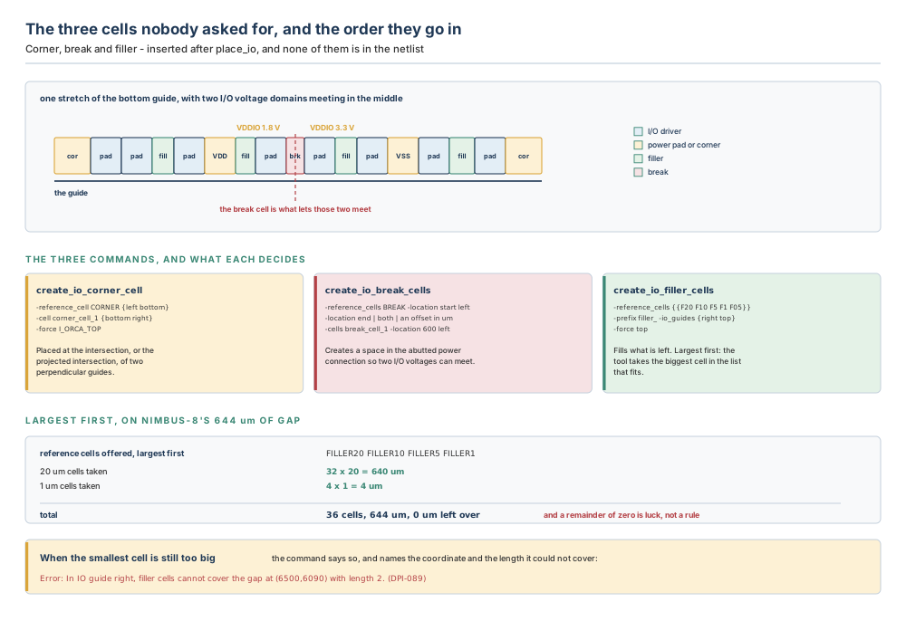
Corner cells are placed at the intersection, or the projected intersection, of two perpendicular guides. -reference_cell inserts a new one from the library; -cell places an instance that already exists; and -force instantiates the cell within a named block, for a design with multiple levels of hierarchy and overlapping blocks.
Break cells create a space between the abutted connections of power nets in the ring, to allow for different voltages. A library might contain several, depending on the supply structure of the drivers and the requirements of the design. -location takes start, end or both to sit just outside one or both ends of a guide, or a distance in microns to move an existing instance that far from the start. Given two guides instead of one, the cell goes at their intersection.
Filler cells populate the empty spaces between driver cells and complete an abutted power connection. Many libraries contain several widths, and the rule that matters is this: when multiple filler references are specified with -reference_cells, the tool chooses the largest possible cell from the list that fills the space. So the list is written largest first, and Nimbus-8's 644 µm of gap per side resolves as
32 × 20 = 640 µm
 4 ×  1 =   4 µm
644 µm in 36 cells, with nothing left over| Option | What it decides | Default if you say nothing |
|---|---|---|
| -reference_cells | The filler references available, written largest first | none |
| -io_guides | Which guides to fill | all of them |
| -prefix | A prefix for the instance names created | none |
| -overlap_cells | Cells the filler may overlap | none |
| -extension_bbox | A bounding box to extend filling into | none |
| -top | Fill at the top level | not specified |
| -block | A list of block path names to fill in | not specified |
| -force | Force the filler into a named block, where a guide overlaps several | not specified |
| -auto_tie_to_pg | Tie the inserted filler to power and ground automatically | not specified |
Verification. check_io_placement -gap, which reports any space between two adjacent cells. And read the command's own output: if the smallest filler is still too big for a remaining gap, it says so and names the coordinate and the length — Error: In IO guide right, filler cells cannot cover the gap at (6500,6090) with length 2.
Common mistakes. Writing the reference list smallest first, so the tool fills a 640 µm gap with 640 one-micron cells. Running filler before break, so the break cell has nowhere to go. Running place_io again afterwards and losing the filler, because place_io removes existing filler cells whose physical_status is not fixed. And filling a ring with no slack in it, which is the Section 6.2.3 mistake arriving three steps late.
6.4.6 RDL: routing, optimising, shielding
After the bump and driver cells are placed, the redistribution layer nets can be routed. The documented procedure is five steps, and the first two are about the rule rather than the router.
# 1. The routing rule. Add -shield_spacings and -shield_widths now
#    if you intend to shield later; they belong on the rule.
icc2_shell> create_routing_rule rdlrule -widths {MRDL 3} \
   -spacings {MRDL 3}

# 2. Collect the RDL nets and apply the rule.
icc2_shell> set rdl_nets [get_nets -of_objects [get_pins \
   -of_objects [get_cells -filter "design_type==flip_chip_pad"]]]
icc2_shell> set_routing_rule [get_nets $rdl_nets] -rule rdlrule
# 3. The routing angle, per layer.
icc2_shell> set_app_options \
   -name flip_chip.route.layer_routing_angles \
   -value {{MRDL 90_degree}}

# 4. Route.
icc2_shell> route_rdl_flip_chip -layers {MRDL}

# 5. Check for open nets, and optionally write an error database.
icc2_shell> report_rdl_routes -open_nets true
icc2_shell> report_rdl_routes -create_error_data verification
Step 2 is worth reading twice. The RDL nets are found by their cells: the flip-chip pads are the cells whose design_type is flip_chip_pad, their pins give the nets, and those nets are the RDL nets. That is the one place in the chapter where the library attribute of Section 6.2.1 is used as a query rather than a requirement — and if a bump's design_type is wrong, this collection quietly comes back short.
| Command or option | What it does | Worth knowing |
|---|---|---|
| route_rdl_flip_chip -layers | Routes the flip-chip nets on the named layers | At most 2 layers, they must be adjacent, and the first is the primary layer |
| route_rdl_flip_chip -skip_detail_route true | Global routing only | Default false. Only one of this and the next may be true. |
| route_rdl_flip_chip -reuse_existing_global_route true | Detail routing only, reusing the existing global route | Default false, and the default deletes all existing global routes before routing starts |
| flip_chip.route.layer_routing_angles | The routing angle per layer: 45_degree or 90_degree | A list of layer-and-angle pairs. Read it back rather than assume it. |
| optimize_rdl_routes -layer -nets | Improves the routing pattern by reducing U- and Z-shaped routes | Creates additional space for RDL power routes |
| optimize_rdl_routes -reserve_power_resources true | Moves signal routes to make room for power and ground | The number of U- and Z-shaped routes might increase |
| route_rdl_differential -mode | length matches route lengths; parallel routes them together in the middle | Default length. At most 16 nets. Do not then run the other RDL commands on that group. |
| split_rdl_routes -mode | adjacent_layer adds a parallel route on the next layer with vias; same_layer splits one route into several thinner ones | Takes -widths, -spacings and -number_of_routes for the same-layer case |
| create_rdl_shields -layers | Creates the shields | Side-wall by default; coaxial with -reference_layer and -offset |
| create_rdl_shields -half_shield | A shield on one side only: up, down, left or right | Default is both sides. Up or down for a horizontal flyline; left or right for a vertical one. |
| create_rdl_shields -shield_on_bump | Whether to shield on the bumps too | Side-wall shielding only |
| create_rdl_shields -trim_floating true | Removes floating shields after creating them | — |
| flip_chip.route.shielding_net | The net the shields connect to | Set it before creating the rule |
| remove_routes -rdl | Removes all RDL routes | Reports how many route shapes it removed |
The angle is worth arithmetic, not opinion. Nimbus-8's longest RDL route runs from a pad centred 60 µm in from the die edge to a bump 520 µm in and 2,850 µm along, so dx is 460 µm and dy is 2,850 µm. At 90 degrees the route is Manhattan and its length is the sum:
460 + 2,850 = 3,310 µmAt 45 degrees the diagonal absorbs the shorter leg, and the length is the longer leg plus 0.414214 times the shorter. That constant is the square root of two, less one, and it is worth keeping in your head: a 45-degree diagonal buys back about 59 per cent of the shorter leg, every time.
2,850 + 0.414214 × 460 = 3,040.5 µm
saving 3,310 − 3,040.5 = 269.5 µm, which is 8.14 per cent
Eight per cent of the wire length on the longest route, from one application option. Whether it is the right choice depends on the technology's rules for diagonal wiring and on whether the RDL is congested — but the size of the prize is arithmetic, and it is worth computing for your own longest route before the discussion starts.
Two more application options are worth knowing by name because their effects are invisible in a summary. flip_chip.route.extend_vias_on_pin takes false, true or full_pin: false makes a simple connection to the pin, true extends the wire and inserts additional stacked vias at the routing rule's width, and full_pin extends and widens the wire to cover the pin, ignoring the rule's width. More vias means lower resistance and better electromigration behaviour; it also means more metal over the pin.
And flip_chip.route.layer_bump_spacings sets the bump-to-route spacing per layer in microns. The same thing can be specified by the technology file rules sameNetRDLMetalToPadMinSpacing and diffNetRDLMetalToPadMinSpacing, and the design rule jogRDLKeepoutRange sets the keepout range between the bump and the route. When a route hugs a bump more closely than you expected, those are the four places to look.
6.4.7 check_io_placement — the nine checks
Purpose. Validate the I/O placement after place_io. The command writes a report listing violating cells and returns a collection of those cells, so it can be used in a script as well as read.
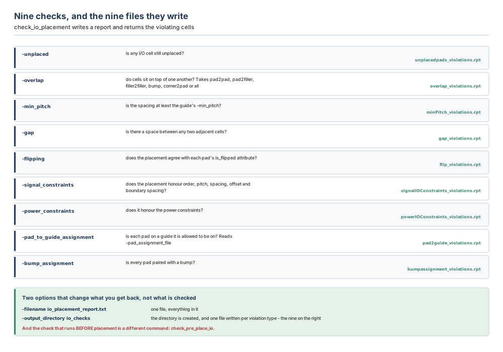
-output_directory and read all nine.The checks divide into three groups. Three are about whether cells are where they should be at all: -unplaced, -overlap and -gap. Three are about whether the placement honours what you asked for: -signal_constraints, -power_constraints and -pad_to_guide_assignment. And three are about consistency with something else: -min_pitch against the guide, -flipping against each pad's is_flipped attribute, and -bump_assignment against the bumps.
Each check prints a bounded report with a start line, the violations, a total and an end line, which makes the output easy to parse and easy to diff between runs. -cells restricts the check to named cells, -io_guides to named guides, and -matching_types to named matching types. -filename writes everything to one file; -output_directory creates a directory and writes one file per violation type — the nine names in Figure 6.10.
Common mistakes. Confusing this command with check_pre_place_io, which runs before placement and checks guides, the pad assignment file and matching types. Reading a total of zero from a command that was given no check options. And treating -gap violations as cosmetic: a gap in the ring is a gap in the abutted power connection.
place_io. Nine checks in the later one, and the option you pass is the check you get — so name them all, or write them all to a directory and read the nine files.6.5 The worked example: Nimbus-8's I/O and bump plan
Eleven steps, in the order Figure 6.1 gave them, on the die Chapter 4 built. Every number has appeared already; this is where they are produced rather than quoted.
Step 0 — check the library, before anything else
# The six attributes of Section 6.2.1, read rather than assumed.
icc2_shell> foreach c {BUMP150 IOPAD46 FILLER20 CORNER110 BREAK20} {
   puts [format "%-12s %s" $c \
      [get_attribute [get_lib_cells */$c] design_type]]
}
BUMP150      flip_chip_pad
IOPAD46      flip_chip_driver
FILLER20     pad_spacer
CORNER110    pad_spacer
BREAK20      pad_spacer
# CORNER110 is wrong: pad_spacer, not corner. Fix it here and
# remember the fix is not propagated to the reference library.
icc2_shell> set_attribute [get_lib_cells */CORNER110] design_type corner

# And the two attributes that are not design_type.
icc2_shell> get_attribute [get_lib_pins */BUMP150/PAD] is_pad
true
icc2_shell> get_attribute [get_lib_cells */IOPAD46] design_type
flip_chip_driver
One of the five was wrong, and that is deliberately realistic. A corner cell delivered as pad_spacer is a plausible library error — corner cells and filler cells are both physical-only, and both sit in the ring — and no command later in this chapter would have told you. create_io_corner_cell would have placed it, and the ring would have looked complete.
Step 1 — the arithmetic, on paper, before the first command
# From Chapter 4, in this chapter's unit.
die                       = 3,440 um on each side
core                      = 3,200 um on each side
core offset (the strip)   =   120 um deep

# From the library.
pad cell                  =   110 um tall, 46 um wide
corner cell               =   110 um on each side
# Does the pad fit the strip?  110 < 120, with 10 um to spare.
guide length  = 3,440 - 2 x 110 = 3,220 um per side

# How many pads, and how much slack?
70 x 46 = 3,220 um  -> exactly full, no slack at all: rejected
56 x 46 = 2,576 um  -> gap of 3,220 - 2,576 = 644 um, 20.0 per cent

# The power pattern, from a ratio of 6 on both cells.
pattern = 6 signal + VDD + 6 signal + VSS = 14 slots
56 / 14 = 4 whole patterns per side
per side = 48 signal + 4 VDD + 4 VSS = 56
ring     = 4 x 56 = 224 pads = 192 signal + 32 power
# From the package.
bump pitch = 150 um
sites across the die: 21 x 150 = 3,150, so 22 sites,
   and (3,440 - 3,150) / 2 = 145 um of margin at each edge
Check each figure backwards before it goes anywhere. 2,576 + 644 = 3,220. 4 × 14 = 56. 192 + 32 = 224, and 32 ÷ 224 = 14.29 per cent while 192 ÷ 224 = 85.71 per cent, which sum to 100. And 145 + 3,150 + 145 = 3,440.
Step 2 — the ring
icc2_shell> create_io_ring -name nimbus_ring -corner_height 110
{nimbus_ring}
icc2_shell> get_io_guides
{nimbus_ring.left nimbus_ring.bottom nimbus_ring.right nimbus_ring.top}
icc2_shell> report_io_guides -verbose
The corner height is stated rather than defaulted, because the default is the tallest pad cell assigned to the ring and no pads are assigned yet. Read the guides back and confirm each is 3,220 µm long.
Step 3 — the bumps, five arrays
# Four signal bands, inline, at the package pitch.
icc2_shell> create_bump_array -lib_cell BUMP150 -delta {150 150} \
   -bbox {{220 220} {520 3070}} -repeat {3 20} -name left
icc2_shell> create_bump_array -lib_cell BUMP150 -delta {150 150} \
   -bbox {{2920 220} {3220 3070}} -repeat {3 20} -name right
icc2_shell> create_bump_array -lib_cell BUMP150 -delta {150 150} \
   -bbox {{895 220} {2545 520}} -repeat {12 3} -name bottom
icc2_shell> create_bump_array -lib_cell BUMP150 -delta {150 150} \
   -bbox {{895 2920} {2545 3220}} -repeat {12 3} -name top

# And one central power and ground field, staggered.
icc2_shell> create_bump_array -lib_cell BUMP150 -delta {150 150} \
   -bbox {{670 670} {2770 2770}} -pattern staggered_1 -name pg_bump
The counts, worked out rather than reported: the left and right bands are 3 × 20 = 60 bumps each, the top and bottom bands 12 × 3 = 36 each, so 2 × 60 + 2 × 36 = 192 signal bumps. The central field is a 15 × 15 grid; staggered_1 keeps the points whose column-plus-row sum is even, and with 8 even and 7 odd indices in 0 to 14 that is 8 × 8 + 7 × 7 = 113. Total 192 + 113 = 305, against 22 × 22 = 484 sites if the die were filled inline — 63.02 per cent of them.
And the number that matters: 192 signal bumps for 192 signal pads. That is the comparison Section 6.3's checklist item 6 asks for, and it comes out to zero difference because the band depths were chosen to make it so.
Step 4 — the constraints
# Power: a ratio of 6 on both reference cells, all four guides.
icc2_shell> set_power_io_constraints \
   -reference_cell {VDD_EW VSS_EW} \
   -ratio {{6 VDD_EW} {6 VSS_EW}} \
   -offset {{100 VDD_EW} {100 VSS_EW}}
Power IO constraints set successfully
# Signal: order from a file, which is the form that scales.
icc2_shell> set_signal_io_constraints -file nimbus_io_order.txt
Signal IO constraints set successfully

icc2_shell> sh cat nimbus_io_order.txt
nimbus_ring.left
{100}
{{order_only}
u_ddr/dq_pad_0 u_ddr/dq_pad_1 u_ddr/dq_pad_2 u_ddr/dq_pad_3}
{40}
{u_isp/pix_pad_0 20 u_isp/pix_pad_1}
;
Two things in that file are worth naming. The bare {100} is an offset — 100 µm from the start of the left guide, which on the left side means 100 µm up from the lower-left corner, because the ordering runs clockwise. And the DDR data pads are constrained order_only, which means their sequence is fixed and their spacing is not: additional spacing and other pad cells might be inserted between them, which is exactly what you want when a power pad has to land in the middle of a byte lane.
Step 5 — matching types, and the check that comes before placement
# Reserve the central field for power and ground: a matching type
# containing only bumps excludes them from signal assignment.
icc2_shell> create_matching_type -name pg_reserved -uniquify 0 \
   [get_cells pg_bump_*]

# Pair one byte lane explicitly, four pads to four bumps.
icc2_shell> create_matching_type -name ddr_byte0 -uniquify 0 \
   {left_0_0 left_0_1 left_0_2 left_0_3 \
    u_ddr/dq_pad_0 u_ddr/dq_pad_1 u_ddr/dq_pad_2 u_ddr/dq_pad_3}

# Check before placing. This is cheap; unpicking afterwards is not.
icc2_shell> check_pre_place_io -matching_types -io_guides
0
The first matching type is the reserved-bumps case from Figure 6.8's gold card, and it is the reason the 113 central bumps do not get signals assigned to them. The second is ordinary pairing. check_pre_place_io returning 0 means all six of its checks passed, including the one that matters most here — that each matching type has enough bumps for the pads in it.
Step 6 — place, then fill
icc2_shell> place_io

# Corners first, then breaks, then filler - filler fills what is left.
icc2_shell> create_io_corner_cell -reference_cell CORNER110 \
   {nimbus_ring.left nimbus_ring.bottom}
icc2_shell> create_io_corner_cell -reference_cell CORNER110 \
   {nimbus_ring.bottom nimbus_ring.right}
icc2_shell> create_io_corner_cell -reference_cell CORNER110 \
   {nimbus_ring.right nimbus_ring.top}
icc2_shell> create_io_corner_cell -reference_cell CORNER110 \
   {nimbus_ring.top nimbus_ring.left}
# Two I/O supply domains meet on the left side.
icc2_shell> create_io_break_cells -reference_cells BREAK20 \
   -location 1610 nimbus_ring.left

# Filler, largest first. The order of this list is the algorithm.
icc2_shell> create_io_filler_cells -prefix filler_ \
   -reference_cells {{FILLER20 FILLER10 FILLER5 FILLER1}}

# Write the placement back out as constraints, so it reproduces.
icc2_shell> write_io_constraints -filename nimbus_io_placed.txt \
   -format spacing
The break cell goes at 1,610 µm from the start of the left guide, which is the midpoint of a 3,220 µm side. The filler then resolves the 644 µm of gap per side as 32 cells of 20 µm and 4 of 1 µm — 36 cells, 644 µm, nothing left over. That remainder of zero is luck rather than a rule; if the library's smallest filler were 5 µm instead of 1 µm, 644 would resolve as 32 × 20 + 0 × 10 + 0 × 5 and leave 4 µm that nothing could cover, and the command would say so.
write_io_constraints -format spacing writes the spacing values between pads along with the pad names. The four documented formats are worth knowing apart: order_only writes only pad order, spacing writes the gaps, pitch writes locations as a cell pitch and requires that all pads be placed evenly in the guide, and fixed specifies that all pad cells are fixed at their current locations.
Step 7 — the RDL, and what the angle is worth
icc2_shell> create_routing_rule rdlrule -widths {MRDL 3} \
   -spacings {MRDL 3} -shield_widths {MRDL 2} -shield_spacings {MRDL 2}
icc2_shell> set rdl_nets [get_nets -of_objects [get_pins \
   -of_objects [get_cells -filter "design_type==flip_chip_pad"]]]
icc2_shell> set_routing_rule [get_nets $rdl_nets] -rule rdlrule

icc2_shell> set_app_options \
   -name flip_chip.route.layer_routing_angles \
   -value {{MRDL 45_degree}}
icc2_shell> report_app_options flip_chip.route.layer_routing_angles

icc2_shell> route_rdl_flip_chip -layers {MRDL} -nets $rdl_nets
icc2_shell> report_rdl_routes -open_nets true
icc2_shell> optimize_rdl_routes -layer MRDL -nets $rdl_nets
# Shields, on the net named by the application option.
icc2_shell> set_app_options -name flip_chip.route.shielding_net \
   -value VSS
icc2_shell> create_rdl_shields -layers {MRDL} -nets $rdl_nets \
   -shield_on_bump true -trim_floating true
The shield widths and spacings go on the routing rule at the moment it is created, not later — that is why they appear in step one of a sequence whose fifth step is the shielding. And report_app_options after setting the angle is the habit this book keeps insisting on: the option's documented values are 45_degree and 90_degree, and reading it back costs nothing.
The angle on Nimbus-8's longest route: from a pad centred 60 µm in from the die edge to a bump 520 µm in and 2,850 µm along the side, dx is 460 µm and dy is 2,850 µm.
at 90 degrees:  460 + 2,850                = 3,310 µm
at 45 degrees:  2,850 + 0.414214 × 460     = 3,040.5 µm
                saving 269.5 µm, which is    8.14 per cent
Step 8 — check what came out
icc2_shell> check_io_placement -output_directory io_checks \
   -unplaced -overlap all -min_pitch -gap -flipping \
   -signal_constraints -power_constraints \
   -pad_to_guide_assignment -bump_assignment
Writing IO placement checking reports to directory io_checks.
icc2_shell> ls io_checks/*
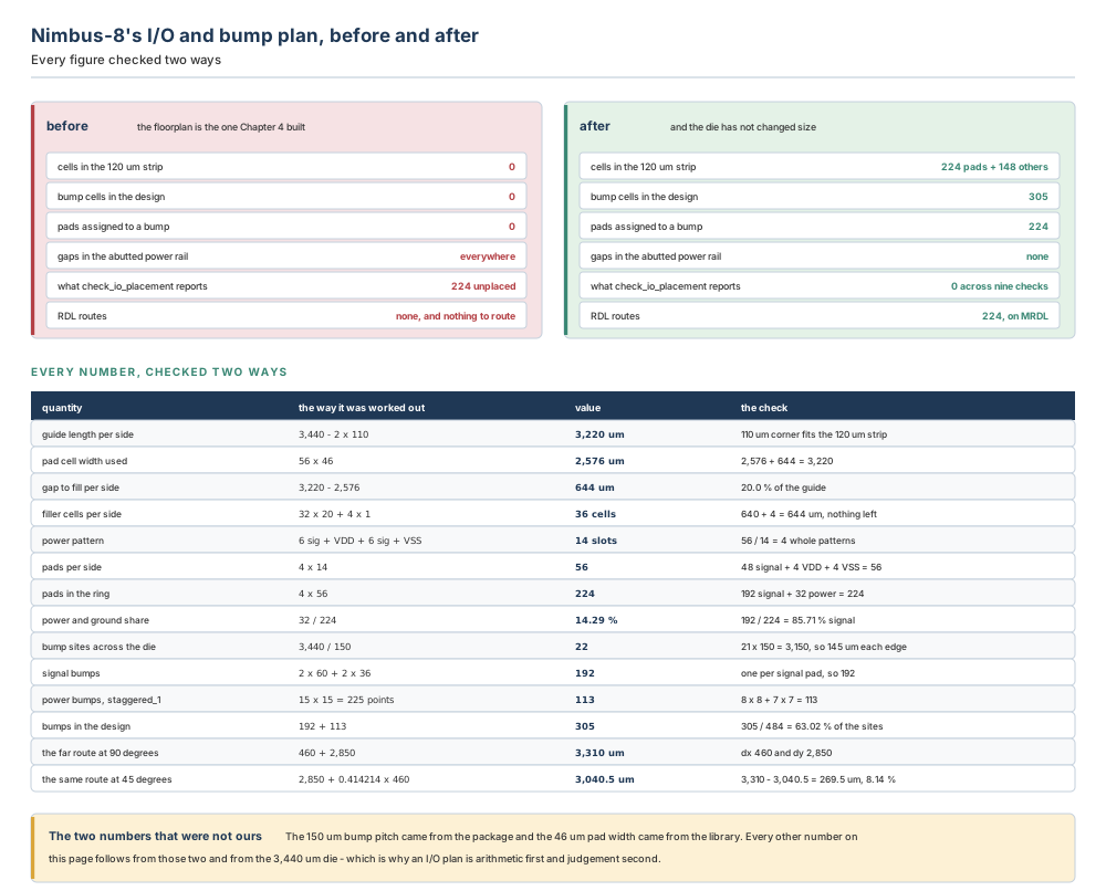
The filler count is worth a sentence, because 4 × 36 = 144 and the figure says 143. Three sides fill 644 µm each, as 32 twenties and four ones, for 36 cells apiece. The left side gave 20 µm of its gap to the break cell, so it fills 624 µm as 31 × 20 = 620 plus 4 × 1 = 4, which is 35 cells. So 3 × 36 + 35 = 143, and 143 + 4 corners + 1 break = 148. Small arithmetic, and exactly the kind that is easier to do now than to reconstruct in a review three weeks later.
Engineering judgement — the four calls that were not the tool's to make
Fifty-six pads and not seventy. The guide holds seventy pads exactly and that is the reason not to use seventy. Twenty per cent slack is a number to defend, not a number to derive; what cannot be defended is discovering at the filler step that there is nowhere to put a break cell.
Fixing the corner cell's design_type in the session. The right fix is in the reference library, and that means a request to whoever owns it. Fixing it here unblocks today's run and nothing more — so the set_attribute line belongs in the setup script with a comment saying why, and the library request belongs in the same commit message.
Choosing the band depths to make 192 equal 192. The first attempt used four bands of 3 × 20, which gives 240 signal bumps for 192 signal pads — 48 bumps with nothing to connect to. Shallower top and bottom bands fixed it. That is the reconciliation Figure 6.1's third panel promised, and it took two attempts because there is no command that does it.
Forty-five degrees rather than ninety. Eight per cent of the longest route is worth having, and the decision still depends on whether the technology's diagonal rules and the RDL congestion allow it. The arithmetic tells you the size of the prize; it does not tell you that you can collect it.
place_io and the RDL router — decide anything by themselves. The other seven are you saying what you worked out on paper first, which is why the paper comes before the prompt.6.6 Failure modes and how to recognise them
Twelve ways this goes wrong. Four produce no message at all, and one of those four points at the wrong part of the design entirely.
| # | What went wrong | How you notice | What to do |
|---|---|---|---|
| 1 | A cell's design_type is wrong in the library. | Nothing. A macro left at its default is simply not considered an I/O cell, so no bumps are assigned to its RDL pins and no command says so. | Read all four values before the first command. Fix with set_attribute to unblock, and raise it against the library — the session fix is not propagated back. |
| 2 | is_pad is not true on a bump cell's library pin. | Terminals for top-level ports are not created automatically when bumps are connected or assigned to ports. The bump looks placed; the port has no terminal. | Set it in the library. This is the one attribute whose absence has a documented, specific consequence, so check it explicitly. |
| 3 | A driver's RDL terminal has no class equal to bump. | A route that works and is wrong. The RDL router chooses the topmost layer terminal of the port instead. There is no violation, just a different connection. | Set class to bump on the intended terminal, or name the terminal in a matching type — the reference recommends the latter. |
| 4 | -side is wrong on a guide. | The pads face into the die. Obvious in the layout and invisible in any report, because a guide with the wrong side is still a valid guide. | Remember that -line is the outer edge and a left guide's pads align on its right. Check one guide in the GUI before creating the other three. |
| 5 | The pad count and the signal bump count do not reconcile. | Nothing, until place_io. Two commands produced two numbers at two different times and nothing compared them. Excess bumps or pad pins simply remain unassigned. | Compare them on paper before running anything. Then fix it by changing the band depths, the pad count, or -uniquify — in that order of preference. |
| 6 | The ring was filled to its exact length. | The filler step has nothing to do and the break cell has nowhere to go. The symptom arrives three steps after the mistake. | Recompute the pad count with slack, and rerun from the ring. Twenty per cent is a reasonable starting point. |
| 7 | The filler reference list was written smallest first. | A 640 µm gap filled with 640 one-micron cells. It is legal, it is slow, and the cell count in the ring is absurd. | Write the list largest first. The tool takes the largest cell that fits, so the order of the list is the algorithm. |
| 8 | place_io was re-run after the filler was inserted. | The filler has gone. place_io removes existing filler cells whose physical_status is not fixed, which happens whenever all pads are considered. | Insert filler last, or fix the filler's physical_status, or re-run the filler step after every placement run. Put it in the script in that order. |
| 9 | -bump_assignment_only was used with constraints set. | The assignment ignores them. In that mode all the signal I/O constraints and power I/O constraints are ignored, by design. | Use it only when you want assignment from current locations. If constraints matter, run a full place_io. |
| 10 | A fixed object sat at the start of a guide. | Pads placed on top of it. By default place_io places pads into the guides and overlaps any existing fixed objects. | Write a constraint file with an absolute constraint and an order-based constraint naming the same first pad. Section 6.4.3. |
| 11 | check_io_placement was run with no check options. | A total of zero, from a command that checked nothing. The option you pass is the check you get. This is the misleading one: the report is not wrong, it is empty, and it looks exactly like a clean ring. | Name all nine checks, or use -output_directory and confirm nine files were written. A zero you cannot account for is a question, not a pass. |
| 12 | The routing angle was never set. | Routes that are longer or shorter than expected, and a discussion nobody can settle because nobody knows which angle was used. | Set flip_chip.route.layer_routing_angles explicitly per layer and read it back with report_app_options. On Nimbus-8 the choice is 8.14 per cent of the longest route. |
Five chapters in, the shape is the same one every time, and Chapter 6 gives it a new variation. Chapter 2's misleading symptom was a setup file that had not been read. Chapter 3's was a constraint file written for a block that never asked for it. Chapter 4's was a re-run that silently deleted routing. Chapter 5's was a clean multivoltage report from a check with nothing to check. This chapter's is a clean placement report from a check that was never asked to check anything.
The pattern is absence reported as success, and the habit that catches all five is the one Chapter 5 named: after a check passes, confirm it examined what you think it examined. Here that is literal. check_io_placement -filename report.txt with no check options writes a report and returns nothing, and the total at the bottom is zero. Count the checks you asked for. Count the files in the output directory. Nine files means nine checks ran.
Chapter 6 adds a second variation worth naming separately, because it is not absence — it is substitution reported as success. A driver terminal with no class equal to bump does not fail to route; the router picks a different terminal and routes to that. The result is a complete, clean, wrong connection. No count will find it. Only reading the assignment back — write_matching_types -from_existing_assignment — will.
6.7 Hands-on mini lab
Goal. Plan the I/O ring and bump field for Fornax-7 from the die outward, reconcile the pad and bump counts before running anything, and quantify what the routing angle is worth.
| Item | Value |
|---|---|
| Die | a square 4,000 µm on each side |
| Core offset (the I/O strip) | 150 µm deep on all four sides |
| Pad cell, from the library | 140 µm tall, 50 µm wide |
| Corner cell, from the library | A square 140 µm on each side |
| Filler cells available | 20 µm, 10 µm, 5 µm, 1 µm |
| Pad slots to fill per side | 60 |
| Power constraint | -ratio 4 on both VDD_EW and VSS_EW |
| Bump pitch, from the package | 200 µm |
| Peripheral signal bands | 3 × 16 on the left and right; 16 × 3 on the top and bottom |
| Central power field | a 13 × 13 grid, -pattern staggered_1 |
| The longest RDL route | dx 425 µm, dy 3,000 µm |
| RDL layer | MRDL |
Tasks.
- Check the strip. Does the pad cell fit the core offset, and by how much? Say what you would do if it did not.
- Compute the guide length, and then how much pad cell 60 slots use and how much gap is left. Give the gap as a percentage of the guide, and check the subtraction by adding back.
- Work out the power pattern. With a ratio of 4 on both cells, how many slots is the repeating unit, how many whole units fit in 60, and how many signal, VDD and VSS pads does each side carry? Then give the whole ring, and the power share as a percentage — twice, from each side of the division.
- Fill the gap. Using the largest-first rule and the four filler widths available, list the cells the gap resolves into and the total count. State whether anything is left over.
- Lay out the bumps. How many sites fit across the die at the package pitch, and how much margin is left at each edge? Then compute the signal bumps from the four bands, and the power bumps from the central grid under
staggered_1— showing the even-and-odd index arithmetic rather than halving. - Reconcile. Compare the signal bump count with the signal pad count. If they differ, say by how much and name the three ways you could close the gap, in your order of preference.
- Cost the angle. Compute the longest RDL route at 90 degrees and at 45 degrees, and give the saving in microns and as a percentage.
- Name the two checks that bracket
place_io, say which runs on which side, and name the one that will report zero violations while having checked nothing.
Expected observations.
1. The pad is 140 µm tall and the strip is 150 µm deep, so it fits with 10 µm to spare — the same margin Nimbus-8 has. If it did not fit there are only two honest options: a shorter pad cell from the library, or a deeper core offset, which means re-running initialize_floorplan and moving the die edge. Neither is a decision to take alone.
2. Guide length 4,000 − 2 × 140 = 3,720 µm. Pad cell used 60 × 50 = 3,000 µm. Gap 3,720 − 3,000 = 720 µm, which is 720 ÷ 3,720 = 19.35 per cent of the guide. Check: 3,000 + 720 = 3,720.
3. A ratio of 4 gives a repeating unit of 4 signal, VDD, 4 signal, VSS = 10 slots. 60 ÷ 10 = 6 whole units. Per side: 6 × 8 = 48 signal, 6 VDD, 6 VSS, and 48 + 6 + 6 = 60. The ring: 4 × 60 = 240 pads = 192 signal + 48 power. Power share 48 ÷ 240 = 20.00 per cent; signal 192 ÷ 240 = 80.00 per cent; the two sum to 100.
4. Largest first on 720 µm: 720 ÷ 20 = 36 exactly, so 36 cells of 20 µm and none of the others, with nothing left over. Worth noticing that this is a cleaner result than Nimbus-8's, which needed four 1 µm cells as well — and that neither outcome was designed, both just fell out of the arithmetic.
5. Sites across: 19 × 200 = 3,800 µm, so 20 sites, with (4,000 − 3,800) ÷ 2 = 100 µm of margin at each edge. Signal bumps: 2 × (3 × 16) + 2 × (16 × 3) = 96 + 96 = 192. Power bumps: a 13 × 13 grid has 7 even and 6 odd indices in 0 to 12, so staggered_1 keeps 7 × 7 + 6 × 6 = 49 + 36 = 85. Total 192 + 85 = 277 bumps, against 20 × 20 = 400 sites — 69.25 per cent used.
6. 192 signal bumps and 192 signal pads: they agree exactly, and the difference is zero. Had they not, the three ways to close the gap, in order of preference: change the band depths, because bumps are cheap to move on paper and the count is the only thing that matters; change the pad count, which means revisiting the slack decision; or use -uniquify to let more than one pad pin share a bump, which is a real mechanism and the last resort because it changes the electrical design rather than the layout.
7. At 90 degrees: 425 + 3,000 = 3,425 µm. At 45 degrees: 3,000 + 0.414214 × 425 = 3,000 + 176.0 = 3,176.0 µm. Saving 249.0 µm, which is 249.0 ÷ 3,425 = 7.27 per cent — slightly less than Nimbus-8's 8.14 per cent, because this route is proportionally straighter.
8. check_pre_place_io runs before and checks guides, the pad assignment file and matching types. check_io_placement runs after and checks the placement, in nine separate checks. The one that reports zero while having checked nothing is check_io_placement, when it is given -filename and no check options at all.
Do task 6 before task 5 on your second pass, and notice how much harder it is. Reconciling two counts is trivial when you have both; deciding what the counts should be so that they will reconcile is the actual work, and it is the work no command in this chapter does for you.
That is the difference between this chapter and Chapter 4. A floorplan can be re-run with different numbers in a minute. An I/O and bump plan is built from a pad width you were given, a bump pitch you were given, and a die somebody else fixed — so the numbers have to be reconciled on paper first, because by the time place_io disagrees with you, four other commands have already run.
6.8 Interview preparation
Sixteen questions, grouped by level. Answer each one out loud before reading the model answer. Flip-chip I/O planning is a favourite interview topic for a practical reason: it is the first part of the flow where a candidate has to reconcile two counts that came from two different organisations, and an interviewer can tell in one question whether you have ever had to do that.
Beginner
BEGINNER
Q1. What does I/O planning add to a design, and in what order?
After creating the floorplan you instantiate the I/O drivers and the bump cells. The flow is: create I/O rings or guides, create bump pad arrays, create power I/O constraints, create signal I/O constraints, create matching types, place the I/O drivers, place the physical-only I/O cells, write the I/O placement constraints, route the RDL nets, optimise the RDL nets, and create the RDL route shields. Two facts make the order make sense rather than just being a list. Guides come first because they are the placement area the drivers get placed into, and nothing can be placed before one exists. Bumps come before drivers because the assignment works from bump positions to driver positions, not the other way round.
What is being tested: whether you can recite a flow in the right order without looking at it. Candidates who have only read about the topic usually put the constraints before the bumps, because that is the order the constraints are written in a script.
BEGINNER
Q2. Before you run any command in this flow, what do you check, and what values do you look for?
You validate that the reference library containing the flip-chip component cells is properly configured, by checking the design_type attribute on four kinds of cell. Bump cells must be flip_chip_pad, and the library cell pin of the bump must have is_pad true. Driver cells must be flip_chip_driver or pad. Filler and break cells must be pad_spacer. Corner cells must be corner. Add the fifth check, which is on a pin rather than a cell: the terminal or pin shape of the driver that is to be connected to an RDL route should have its class attribute set to bump. And say why is_pad matters — you must set that attribute for the tool to create terminals for top-level ports automatically when bumps are connected or assigned to ports.
What is being tested: whether you check anything at all before the first command. This is the one step in the chapter with no command of its own and no report, and it is the step whose omission produces the most confusing downstream symptoms.
BEGINNER
Q3. What is an I/O guide, what is an I/O ring, and how do you make one?
An I/O guide forms a placement area for I/O drivers. A ring is four guides along the periphery of the floorplan. You can create the ring either with four create_io_guide commands, one per side, or with a single create_io_ring command. Multiple rings and multiple guides on the same side of the die are both supported. The detail worth volunteering is that create_io_ring -name uses the name as a prefix, so a ring called nimbus_ring yields the guides nimbus_ring.left, nimbus_ring.bottom, nimbus_ring.right and nimbus_ring.top, retrievable with get_io_guides. That naming is what every later constraint refers to, so it is not cosmetic.
What is being tested: whether “ring” and “guide” are separate objects in your head. They are separate object types with separate creation, reporting and removal commands, and the constraint commands take guides, not rings.
BEGINNER
Q4. A colleague gives you an ordered list of pads for the top edge. Where does that order start?
Signal ordering begins at the lower-left pad for the left edge, the upper-left pad for the top edge, the upper-right pad for the right edge, and the lower-right pad for the bottom edge. Say the shape rather than the four cases: the four start points go round the die clockwise, and each side runs from its own start towards the next corner. So the top edge runs left to right, the right edge runs top to bottom, the bottom edge runs right to left, and the left edge runs bottom to top. Volunteer what to do with the answer — read the placement back, or write it out with write_io_constraints, and confirm the first pad in the list ended up at the corner you expected.
What is being tested: whether you know the ordering is per-side and not global. A candidate who assumes every side runs left to right and bottom to top gets two sides of the die reversed, and both of them place cleanly with no violation reported.
Intermediate
INTERMEDIATE
Q5. Explain the three bump array patterns, and say how many bumps each produces on a grid.
The -pattern option of create_bump_array takes inline, staggered_1 or staggered_2. The inline keyword, which is the default, places bump cells at each point in the array specified by -delta. The staggered_1 keyword places bump cells at points where the sum of the column index and the row index is even. The staggered_2 keyword places them where that sum is odd. Then do the counting out loud, because the interviewer is waiting for it. On a grid of c columns and r rows, inline gives c × r. A staggered pattern does not give exactly half unless both counts are even: on a 15 by 15 grid the indices 0 to 14 hold eight even values and seven odd ones, so staggered_1 keeps 8 × 8 + 7 × 7 = 113 of the 225 points, which is 50.2 per cent rather than 50. On an even grid the two staggered patterns give the same count; on an odd one they differ by the number of rows or columns.
What is being tested: whether “staggered means half” is a rule or an approximation in your head. Interviewers who have counted bumps for a power budget ask for the number, not the description.
INTERMEDIATE
Q6. What do -ratio, -spacing, -offset and -share mean on set_power_io_constraints?
Different units, which is the whole point of the question. -ratio defines the number of signal pads that can be placed between successive power pads, so it counts pads. -spacing specifies the maximum spacing between successive power pads of the same type, in microns. -offset specifies the maximum distance between the starting point of the I/O guide and the closest edge of the first power pad of the specified type, also in microns. -share assigns more than one power pad to a given bump cell, so it counts pads per bump. The pattern to say out loud: two of these four count objects and two measure distance, and the two that count are the two whose numbers look most like distances in a script. And note the shape of the values — each is a list of pairs of a number and a reference cell, as in -ratio {{7 VDD_NS} {6 VSS_NS}}, so the constraint is per cell type and not per guide.
What is being tested: unit awareness. Writing -ratio 150 when you meant a 150 µm spacing is a legal command that asks for 150 signal pads between power pads, and on any real side that means the constraint never binds.
INTERMEDIATE
Q7. Give me the constraint formats set_signal_io_constraints accepts.
Four shapes inside -constraint. {{order_only} pad_1 pad_2 ...} places the pads in the specified order, and additional spacing and other pad cells might be inserted between adjacent pads. Bare spacing values interleaved with the names, as in {pad_1 10 pad_2 20 pad_3}, insert a 10 µm space between the first two pads and a 20 µm space between the next two. {{pitch} pad_1 pad_2 ...} places each driver at a specified pitch. And {{absolute} pad_iopad_1 200.0} places one named pad at a fixed distance from the start of the guide. Two more mechanisms belong in a full answer. A bare number on its own line in a constraint file, such as {80}, is an offset from the start of the guide to the next pad. And for a large number of constraints you write them out with write_io_constraints -filename and load them with set_signal_io_constraints -file, or supply a CSV file with -csv, where only the “Pad Name” field is required, “Offset Value” is optional, other fields are read and ignored, fields may appear in any order but must not repeat, and every row must have the same number of fields. Custom column headings are mapped to the standard ones with -map_file.
What is being tested: whether you know that order and spacing are separate concerns that compose. Candidates who only know order_only cannot express a bus that needs a fixed pitch, and candidates who only know spacing values cannot express “these four, in this order, wherever they fit”.
INTERMEDIATE
Q8. Compare automatic bump assignment with matching types. Which do you use?
Both are supported. Automatic assignment is place_io -bump_assignment_only: the tool does only bump assignment, no pad placement is done, I/O driver cells are not moved, and bumps are assigned based on the current locations of the drivers. User-specified assignment is create_matching_type: the tool assigns flip-chip drivers to flip-chip bump cells that have the same matching type, and -uniquify specifies the number of pad pins that can be assigned to a single bump cell, with 0 meaning each bump cell can be assigned to only one pad cell. The tradeoff, stated as a tradeoff. Automatic assignment is right when nothing about the pairing matters beyond “short” — most single-ended signals, most of the time — and it is fast, complete and needs no maintenance. Matching types are right when the pairing itself is a requirement: a differential pair that must land on adjacent bumps, a bus whose bit order must survive into the package, a group of bumps reserved for power. Matching types cost you a file to maintain and a check to run, and they silently narrow what place_io will touch.
How I would answer the “which”: automatic first, then inspect. Run place_io -bump_assignment_only, write the result out with write_matching_types -from_existing_assignment -file_name, read that file, and convert to explicit matching types only the groups where the automatic answer was wrong or where the pairing is a contract with somebody else. That gives you a small hand-maintained set instead of a large one, and the tool's own output as the starting point.
What is being tested: whether you treat the two as exclusive. They are not: the automatic assignment can be written out as matching-type commands and sourced back, which makes “automatic, then edit” a real workflow rather than a compromise.
INTERMEDIATE
Q9. There are two special kinds of matching type. What are they and what is each for?
The first contains only bumps. Those bumps are excluded from bump assignment and are not connected to any pad pins, unless they were already connected to bumps in the original netlist by two-pin nets. Use this to reserve bump cells for power or ground and avoid connecting them to I/O driver cells. The second contains no bumps at all — only drivers, driver pins or driver terminals. Those pads are excluded from I/O placement, remain at their current position, and are not processed during bump assignment. Both are worth knowing because both look like mistakes in a script. A matching type with no pads reads like an unfinished line, and a matching type with no bumps reads like a forgotten one. They are the documented mechanisms for “hands off these bumps” and “hands off these pads”, and there is no other way to say either.
What is being tested: whether you have read past the common case. This is also the answer to the practical question “how do I stop the tool assigning a signal to my power bumps”, which comes up on every flip-chip design.
INTERMEDIATE
Q10. Which cells do you insert after place_io, and how does the tool pick a filler?
Three commands. create_io_corner_cell places corner cells at the intersection or projected intersections of two perpendicular I/O guides. create_io_break_cells creates a space between the abutted connections of power nets in the I/O ring to allow for different voltages, positioned with -location start, end, both, or a distance in microns from the start of a named guide. create_io_filler_cells populates the empty spaces between driver cells and completes an abutted power connection. When multiple filler references are given with -reference_cells, the tool chooses the largest possible cell from the list that fills the space. Say the two consequences of that last sentence. First, order the list largest to smallest and include a cell small enough for your remainder, or you get an error naming a gap the fillers cannot cover — the message reports the coordinate and the length. Second, work out the fill on paper: a 644 µm gap with 20, 10, 5 and 1 µm cells is 32 twenties and four ones, with nothing left, which is only knowable if a 1 µm cell exists in the library.
What is being tested: whether “filler” sounds optional to you. The abutted power connection along the ring is not complete until the gaps are closed, so this is a connectivity step wearing the costume of a cosmetic one.
INTERMEDIATE
Q11. Compare check_pre_place_io and check_io_placement.
Different times and different subjects. check_pre_place_io -matching_types runs before placement and checks the constraints you wrote: top-level matching type consistency; that matching types do not contain bump cells, bump pins or bump terminals at lower levels of hierarchy; that each object has only one matching type; that each matching type has enough bumps for bump assignment; netlist violations, since components within the same matching type must be connected to the same net or be unconnected; and matching type agreement across all multiply instantiated block instances. check_io_placement runs after place_io and checks the result, writing a report of violating cells and returning a collection of them. Name the nine after-checks in three groups rather than as a flat list. Are the cells where they should be at all: -unplaced, -overlap — which takes pad2pad, pad2filler, filler2filler, bump, corner2pad or all — and -gap. Does the placement honour what you asked for: -signal_constraints, -power_constraints and -pad_to_guide_assignment. And is it consistent with something else: -min_pitch against the guide, -flipping against each pad's is_flipped attribute, and -bump_assignment against the bumps. -cells, -io_guides and -matching_types narrow the scope rather than adding a check, and -output_directory writes nine separate violation files, one per type, which is the artefact to keep for a review.
The tradeoff: the before-check is cheap and finds contradictions in your intent; the after-check is the only one that sees what actually happened. Running only the second means debugging a placement that was impossible to satisfy; running only the first means trusting that a satisfiable request was satisfied. Both, every time, and the second one with explicit check options.
What is being tested: whether you know the second command checks nothing by default. Options control which checks are performed, so check_io_placement -filename report.txt writes a clean report having examined nothing.
Senior
SENIOR
Q12. What would you do if the package team hands you fixed bump locations and their count disagrees with your pad count?
Read the locations in rather than recreating them — read_aif takes a list of bump cells and locations from an AIF or DEF file, with -hierarchy if the file also carries I/O pad locations to place in any level of physical hierarchy. Then reconcile the two counts on paper before running anything else, because place_io will not reconcile them for you: excessive bumps or pad pins simply remain unassigned. The order in which I would try to close the gap, and why. If there are more bumps than pads, that is usually fine and often deliberate — reserve the surplus with a bumps-only matching type so nothing gets assigned to them, and confirm with the package team which ones are theirs. If there are more pads than bumps, the options in order of preference are: reduce the pad count, which means revisiting whichever design decision produced it; let more than one pad pin share a bump with -uniquify or, for power, -share, which is a real mechanism and changes the electrical design; or go back and ask for a different bump map, which is the honest answer when the shortfall is large and the earliest possible request. What I would not do is run place_io and read the count off the result, because the command's behaviour on a mismatch is to leave things unassigned, not to complain.
What is being tested: whether you volunteer the reconciliation, or wait to be told. The interviewer usually knows the count already; they want to hear the sequence “count both, compare, decide, then run”.
SENIOR
Q13. What would you do if some of the I/O pads live inside a block rather than at the top level?
The tool supports top-level and block-level flip-chip planning for designs with multiple levels of physical hierarchy, and top-level flip-chip routing connects bump cells at the top level and ignores bump cells within the blocks. The rules I would work to: blocks containing I/O bump cells or pad cells must be preplaced; I/O pad cells may be at the top level or the block level, and block-level ones are considered fixed; I/O guides are created at the top level; matching types assigning top-level bumps to block-level I/O cells must be created at the top level; and block-level I/O pads should be specified with create_matching_type. Add the fallback and the guide rules. For block-level pads not named in a matching type, the pin shapes should have their class attribute set to bump, which is the second route to the same outcome and the one that fails silently if the library was never prepared. On guides, remember that all flip-chip bump cells must be placed at the top level, guides are not allowed to cross block boundaries for a placed block, I/O pad cells and their guide must be in the same physical block instance, only pads in the same logical hierarchy as the guide can be constrained with set_signal_io_constraints, and guides must not overlap.
What is being tested: whether you know which objects are top-level-only. Bumps and guides are; pads are not. A candidate who tries to create a bump array inside a block has not read the constraint, and the resulting design looks plausible until top-level routing ignores those bumps.
SENIOR
Q14. What would you do if route_rdl_flip_chip finishes and some nets are open?
Find out which, first: report_rdl_routes -open_nets true lists the open nets by name, and report_rdl_routes -create_error_data verification writes an error database for the Error Browser covering both opens and shorts, with the flyline_only keyword available if I only want the flyline data. Then work down the causes in the order that costs least to check. Was the net assigned at all — an open net with no flyline was never paired, which is a matching-type or design_type question, not a routing one. Is there room — the bump-to-route spacing set by flip_chip.route.layer_bump_spacings, the jogRDLKeepoutRange design rule, and the route width and spacing in the routing rule together decide whether a channel exists between two bumps at all. Is the geometry available — a 90-degree setting on a diagonal-dominated field asks for staircases where a 45-degree one asks for a straight line. And is the connection at the pin end being made where I think it is: if the driver has no terminal with class set to bump, the RDL router chooses the topmost layer terminal of the port instead, which routes cleanly to the wrong place rather than failing.
What I would try before re-routing everything: optimize_rdl_routes to reduce the U- and Z-shaped routes, which is often what closed the channel; split_rdl_routes where one wide route has to become several thin ones on the same layer or a parallel route on an adjacent layer; and only then a change to the rule or the angle, since those re-route the whole field.
What is being tested: whether you distinguish “not routed” from “not assigned”. They present identically in a layout view and have nothing in common.
SENIOR
Q15. Ninety-degree or forty-five-degree RDL routing? And side-wall or coaxial shielding?
Both are set before routing, not after. The angle comes from flip_chip.route.layer_routing_angles, set per layer to 90_degree or 45_degree, and it is read by route_rdl_flip_chip. Shielding style comes from the commands: create_rdl_shields does side-wall shielding on the same layer or coaxial shielding above and below the layer, and coaxial shielding provides better signal isolation than side-wall shielding but uses more routing resources. On the angle, do the arithmetic rather than asserting a preference. A route with a 460 µm horizontal offset and a 2,850 µm vertical one is 460 + 2,850 = 3,310 µm as two orthogonal legs, and 2,850 + 0.414214 × 460 = 3,040.5 µm if the diagonal part is taken at 45 degrees — a saving of 269.5 µm, or 8.14 per cent. The saving is largest when the two offsets are similar and vanishes when one dominates, so it is worth measuring on your own worst net before deciding. Against it: 45-degree routes are harder to check by eye, harder to shield neatly, and not every fabrication flow downstream is equally happy with them.
On shielding: side-wall costs one track either side of the net and is what -shield_widths and -shield_spacings in the routing rule size; coaxial costs a layer above or below and needs -reference_layer and -offset, with the target and reference layers necessarily different. Side-wall has two options coaxial does not — -shield_on_bump and -half_shield with up, down, left or right — and half-shielding is the honest middle option when resources are short. I would shield the few nets that need it coaxially rather than shielding everything side-wall, and I would set flip_chip.route.shielding_net deliberately rather than discovering afterwards what the shields were tied to.
What is being tested: whether you have an opinion with a number behind it. “45 degrees is shorter” is true and useless; “8.14 per cent on our worst net, and here is what it costs us in checking” is an engineering answer.
SENIOR
Q16. What would you do if the I/O plan looks clean and you do not believe it?
Distrust the reports that can be clean for the wrong reason, and check the three things this chapter can get wrong without complaining. One: check_io_placement with no check options performs no checks, so re-run it with the options named explicitly and -output_directory, then confirm nine violation files exist and read the ones you did not expect to be empty. Two: a driver whose terminal has no class set to bump gets routed to the topmost layer terminal of the port instead, cleanly. Three: a macro's default design_type is macro and bump assignment is not performed for macros, so a macro pin needing a bump has to be in a matching type — explicitly including the pin is the recommended methodology. Then the arithmetic audit, because the numbers are the part no command validates. Recount the guide length from the die and the corner height. Recount the pads that fit from the guide length and the pad width, and confirm the leftover matches what the fillers can cover exactly. Recount the signal bumps against the signal pads and confirm the difference is zero or deliberate. Recount the bump sites from the pitch and the die, and check the margin at the die edge adds back. Finally, write the placement out with write_io_constraints and read it as a human: the file lists the pads in guide order, so the order you intended is directly visible, and a reversed side is obvious in text in a way it is never obvious in a layout view.
The habit behind the answer: everything in this chapter is either a number somebody else fixed, a number that follows from those by arithmetic, or a decision you made. The tool checks the third category against the first two. Nobody checks the arithmetic but you.
What is being tested: whether you can name a specific way a clean report lies. Every senior candidate says they are sceptical; the ones who have been burned name the option that made the report empty.
6.9 Chapter close
Sign-off checklist
- The library has been validated:
design_typeisflip_chip_padon bumps withis_padtrue on the bump pin,flip_chip_driverorpadon drivers,pad_spaceron filler and break cells, andcorneron corner cells. - Every driver terminal that an RDL route must reach has its
classattribute set tobump, and every macro pin that needs a bump is named in a matching type. - The guide length per side has been computed from the die size and the corner height, and the corner cell fits inside the core offset the floorplan reserved.
- The pad count per side has been computed from the guide length and the pad width, with slack deliberately left over rather than discovered.
- The leftover gap on each side is covered exactly by the available filler widths, largest first, with nothing remaining.
- The power pattern has been written out as a repeating group of slots, the whole number of repetitions per side checked, and the resulting power share of the ring recorded.
- Signal ordering has been supplied per side, with the start corner of each side confirmed, and the placement read back and compared against it.
- The bump pitch and any fixed bump locations came from the package, are recorded as such, and were read in rather than recreated.
- The bump count per array has been computed from the pattern and the grid, and the total compared against the number of sites the die holds.
- The signal bump count and the signal pad count have been compared, and any difference is deliberate and written down.
- Bumps reserved for power or ground are protected by a bumps-only matching type, and pads that must not move are protected by a matching type with no bumps.
check_pre_place_io -matching_typeshas run clean before placement.check_io_placementhas run with every check option named explicitly and-output_directory, and all nine violation files have been read.- Corner, break and filler cells have been inserted, and no gap remains in the abutted power connection.
- The RDL routing angle, bump-to-route spacing, shielding net and via extension have been set deliberately and read back with
report_app_options. report_rdl_routes -open_nets truereports nothing, and the placement has been written out withwrite_io_constraintsand kept.
Flashcards
Guides, bumps, power constraints, signal constraints, matching types, place_io, physical-only cells, write constraints, route RDL, optimise RDL, shield RDL.
design_type valuesflip_chip_pad bumps, flip_chip_driver or pad drivers, pad_spacer filler and break, corner corners.
is_pad true on the bump cell's library pin; class set to bump on the driver terminal the RDL route must reach.
Lower-left for left, upper-left for top, upper-right for right, lower-right for bottom. Clockwise.
The die side less two corner heights. Everything else on that side follows from it.
-delta and -lib_cell. The pitch is -delta, and it came from the package.
inline every point, staggered_1 where column plus row is even, staggered_2 where it is odd.
-ratio counts signal pads, -share counts pads per bump. -spacing and -offset are microns.
{{order_only} p1 p2 p3}, interleaved spacing values as in {p1 10 p2 20 p3}, {{pitch} p1 p2 p3}, and {{absolute} p1 200.0}.
-uniquify meansThe number of pad pins that can be assigned to a single bump cell. Zero means one pad per bump.
Bumps only reserves those bumps. Pads only excludes those pads from placement and assignment.
-bump_assignment_only ignoresAll signal and power I/O constraints. It assigns from current driver locations and moves nothing.
The largest possible cell from the list that fills the space. Order the list largest first and include a small one.
check_pre_place_io -matching_types, six checks. check_io_placement, nine checks, none of them by default.
flip_chip.route.layer_routing_angles, per layer, 90_degree or 45_degree. Set it before routing.
Coaxial isolates better and costs more routing resources. -shield_on_bump and -half_shield are side-wall only.
Compact glossary
| Term | Meaning as used in this book |
|---|---|
| AIF file | A package description carrying die size and a list of bump names with x- and y-coordinates, read with read_aif. The mechanism by which the package fixes the bump map. |
| Break cell | A physical-only cell that creates a space between the abutted connections of power nets in the I/O ring, to allow for different voltages. design_type pad_spacer. |
| Bump array | A grid of bump cells created by create_bump_array inside a bounding box or boundary, spaced by -delta and populated according to -pattern. |
| Bump cell | The cell the package solders to. design_type flip_chip_pad, with is_pad true on its library cell pin. All flip-chip bump cells must be placed at the top level. |
| Bump pattern file | The input to create_bump_pattern, defining the bump library cell, the pitch, the I/O groups, orientation, offsets, spacings and matching type prefixes. Used where pads are not placed with guides. |
| Coaxial shielding | Shielding a net above and below its layer. Better isolation than side-wall shielding, and more routing resources. Needs -reference_layer and -offset. |
| Corner cell | A physical-only cell placed at the intersection, or projected intersection, of two perpendicular I/O guides. design_type corner. Its height sets how much of each side the ring loses. |
| Driver cell | The cell that shifts a signal on or off the die. design_type flip_chip_driver or pad, or macro if flip-chip matching types are defined. |
| Filler cell | A physical-only cell populating empty space between drivers and completing the abutted power connection. design_type pad_spacer. Selected largest-first from the reference list. |
| I/O guide | A placement area for I/O drivers. Guides must not overlap, must not cross the boundary of a placed block, and must share a physical block instance with their pads. |
| I/O ring | Four I/O guides along the periphery of the floorplan. Created by one create_io_ring or four create_io_guide commands; the ring name prefixes the guide names. |
| Matching type | A named group used for driver-to-bump pairing and for driver placement. Drivers are assigned to bump cells with the same matching type, in the ratio given by -uniquify. |
| Pitch, bump | The centre-to-centre spacing of the bump grid, given to create_bump_array as -delta or to a bump pattern file as bump_pitch. A package constraint, not a choice. |
| RDL | The redistribution layer, or layers, on which routes join driver terminals to bump cells. Routed by route_rdl_flip_chip, improved by optimize_rdl_routes, shielded by create_rdl_shields. |
| Ratio, power I/O | The number of signal pads that can be placed between successive power pads of one reference cell. A count of pads, not a distance. |
| Share, power I/O | The number of power pads allowed to drive a single bump cell, per reference cell. Also a count, not a distance. |
| Side-wall shielding | Shielding a net on its own layer, on both sides by default. Sized by -shield_widths and -shield_spacings in the routing rule; -half_shield restricts it to one side. |
| Staggered pattern | A bump array occupying alternate grid points: staggered_1 where the column and row indices sum to an even number, staggered_2 where they sum to an odd one. |
| Uniquify number | The -uniquify value of a matching type: how many pad pins may be assigned to one bump cell. Zero restricts each bump cell to a single pad cell. |
| Virtual I/O guide | What the tool creates for a group of pad cells that are not inside any I/O guide, so that they can still be placed and assigned. |
Five-question self-check
A new design, Vela-3. The die is a square 2,800 µm on each side. The corner cell is 100 µm high, the signal pad is 40 µm wide, the filler library holds 20, 10, 5 and 1 µm cells, and the package specifies a 180 µm bump pitch.
- How long is each I/O guide, how many 40 µm pads would fit end to end, and if you decide to place 50 pads per side, how much gap is left and what fraction of the guide is that?
- You set a power ratio of 4. Write out the repeating pattern of slots, say how many whole patterns fit into the 50 slots, and give the signal, VDD and VSS pad counts per side and the power share of the whole ring.
- Fill that leftover gap largest-first from the 20, 10, 5 and 1 µm cells. How many cells, of which sizes, and how much is left over?
- At a 180 µm pitch, how many bump sites fit across the 2,800 µm die, and how far is the outermost bump centre from the die edge? Then: how many bumps does
staggered_1place on an 11 by 11 grid? - A route has to cover 380 µm horizontally and 2,400 µm vertically. Give its length at 90 degrees and at 45 degrees, the saving, and the saving as a percentage.
Answers.
1. Guide length is the die side less two corner heights: 2,800 − 2 × 100 = 2,600 µm. Pads that fit end to end: 2,600 ÷ 40 = 65 exactly. At 50 pads: 50 × 40 = 2,000 µm of pad, leaving 2,600 − 2,000 = 600 µm, which is 600 ÷ 2,600 = 23.08 per cent of the guide. Check backwards: 2,000 + 600 = 2,600, and 2,600 + 200 = 2,800. Note that 65 is what fits, not what you would place — 50 is the number you chose, and the 600 µm is the slack you chose to keep.
2. A ratio of 4 means no more than four signal pads between successive power pads of that type, so the repeating pattern is four signal, VDD, four signal, VSS — ten slots. 50 ÷ 10 = 5 whole patterns, with nothing left over. Per side that is 5 × 8 = 40 signal, 5 VDD and 5 VSS, and 40 + 5 + 5 = 50. Round the ring: 4 × 50 = 200 pads, of which 4 × 10 = 40 are power. Power share 40 ÷ 200 = 20.00 per cent, signal 160 ÷ 200 = 80.00 per cent, and the two sum to 100.
3. 600 ÷ 20 = 30 exactly, so 30 cells of 20 µm, none of the others, and nothing left over. Worth noticing that this outcome depends entirely on the numbers: 600 happens to be a multiple of 20, whereas Nimbus-8's 644 µm needed 32 twenties and four ones. Neither result was designed. Both had to be checked.
4. Sites across: 2,800 ÷ 180 = 15.56, so 15 sites — each site takes a pitch-wide slot, and a sixteenth slot does not fit. Fifteen sites means fourteen gaps, spanning 14 × 180 = 2,520 µm of centre-to-centre distance, which leaves 2,800 − 2,520 = 280 µm to share between the two edges, so the outermost bump centre sits 140 µm from each die edge. Check: 140 + 2,520 + 140 = 2,800. On an 11 by 11 grid the indices 0 to 10 hold six even values and five odd ones, so staggered_1 places 6 × 6 + 5 × 5 = 36 + 25 = 61 bumps of the 121 grid points, which is 50.4 per cent — not half, because the grid is odd on both axes.
5. At 90 degrees the route is two orthogonal legs: 380 + 2,400 = 2,780 µm. At 45 degrees the diagonal part replaces the shorter leg: 2,400 + 0.414214 × 380 = 2,400 + 157.4 = 2,557.4 µm. Saving 222.6 µm, which is 222.6 ÷ 2,780 = 8.01 per cent. Close to Nimbus-8's 8.14 per cent, and for the same reason — in both cases one offset dominates the other by roughly six to one, so the diagonal has little room to help. The lesson is the one to carry: the saving is a property of the geometry of your worst net, not a property of the option, so measure it before you argue for it.
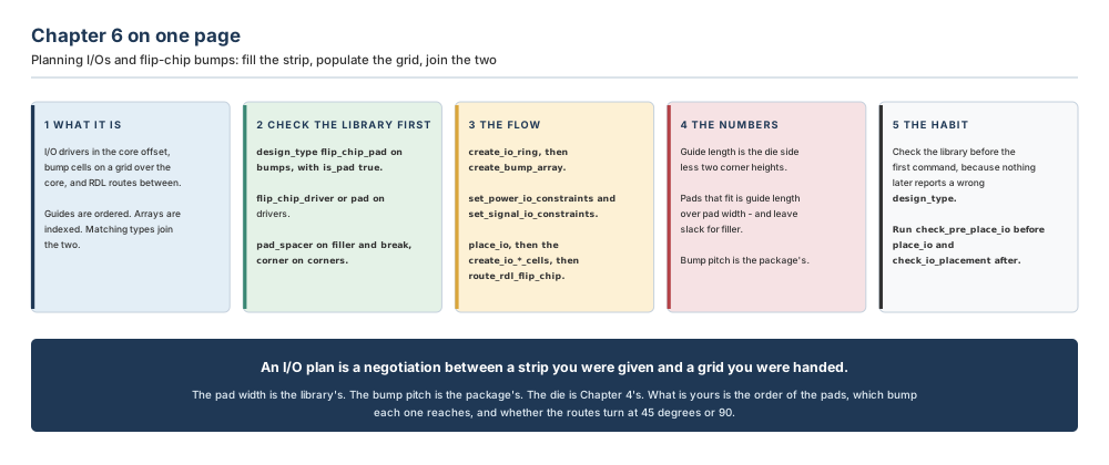
Where the next chapter goes, and why
The strip that Chapter 4 reserved is now full. Drivers sit in ordered positions inside four guides, power pads appear at a stated frequency, corner cells hold the four intersections, filler closes every gap in the abutted power connection, a field of bumps covers the die at the package's pitch, and every driver that needs one reaches a bump through a route you can measure. The design has an outside world for the first time.
What is still true is that it is one die. Everything so far — the boundary, the rows, the tracks, the blocks, the black boxes, the ring and the bump field — describes a single piece of silicon with a package on top of it. Chapter 7 removes that assumption. In a 3DIC design two or more die are stacked vertically to make one system, and in a 2.5D design one or more die are mounted on an interposer that connects them to each other and to the package, an interposer that may be silicon or glass.
The link back to this chapter is direct and worth holding on to. A bump is where one piece of silicon hands a signal to something outside itself, and this chapter was about planning that handover when the something outside is a package. Stacking changes what is on the other side, not the nature of the problem: there is still a grid of connections whose pitch somebody else fixed, still a count on each side that has to reconcile, and still an assignment that nothing downstream will tell you was wrong.