CHAPTER ONE
What a Design Plan Is, and Why the Rest of the Chip Obeys It
By the end of this chapter you will be able to explain what design planning produces, decide how a large netlist should be divided into physical blocks, size a core from cell area, and prove that a design is ready for the next planning step instead of hoping that it is.
Why this chapter matters in a real project
On a large chip, the decisions made in the first week of physical work are the ones nobody gets to take back cheaply. Where you draw the boundary between two blocks decides how many wires must cross that boundary for the next nine months. How big you make the core decides how much silicon area the company pays for on every wafer, forever.
Design planning is the stage where those decisions are made deliberately rather than by accident. It sits between synthesis, which produced a netlist with no physical meaning at all, and implementation, which will spend enormous compute on placement, clock trees and routing. Its job is not to finish anything. Its job is to find out — quickly, and before the expensive steps start — whether the shape of the chip you have in mind can actually work, and to hand every downstream team a piece of the problem small enough to solve.
Engineers who are good at this stage look slow at first. They measure before they draw. They write down the assumption behind every number. They run a cheap check before a long command. Then they finish months earlier than the engineer who started by typing a die size.
Prerequisites
This is the first chapter, so it assumes only that you know what a logic gate and a flip-flop are, and that a netlist is a list of cells and the nets connecting them. Everything physical is introduced from zero; if you have never seen a floorplan, a routing track or a Tcl command, you are the reader this chapter was written for.
Learning objectives
- State in one sentence what design planning produces and what decision it exists to support.
- Distinguish die from core, logical from physical hierarchy, and a hard macro from a standard cell.
- Compute a core area from a cell count, an average cell area and a target utilisation, and state the result with units.
- List the four factors that decide where a partition boundary goes, and apply them to a module list.
- Explain what changes in the design database when a logical module is committed to a physical block.
- Explain why a multiply instantiated block constrains pin placement, and what a feedthrough is.
- Name the validation keyword that guards each planning step, and run the pre-floorplan check on a design.
- Diagnose a failed planning step from its message summary rather than from its first line.
1.1 The beginner’s mental model
Start with a building
An architect handed an empty plot and a list of requirements — twelve offices, one laboratory, a server room, a lift — does not begin by drawing walls. She begins by adding up how many square metres of room she has been asked for, comparing that with the plot, and deciding how the space will be divided. Only then does she draw. She knows that corridors are not wasted space: without them nobody reaches the offices. She knows the lift shaft cannot be moved to suit a nicer layout, because it is a fixed structure that arrives as it is. And she knows that if she gets the division wrong, every later drawing inherits the mistake.
Design planning is that stage of work for a chip. You are handed a netlist instead of a room list, silicon area instead of a plot, and hard intellectual-property blocks instead of a lift shaft — and the discipline is the same. Measure, divide, place the immovable things, leave room for the connections, and check the arithmetic before anyone starts building.
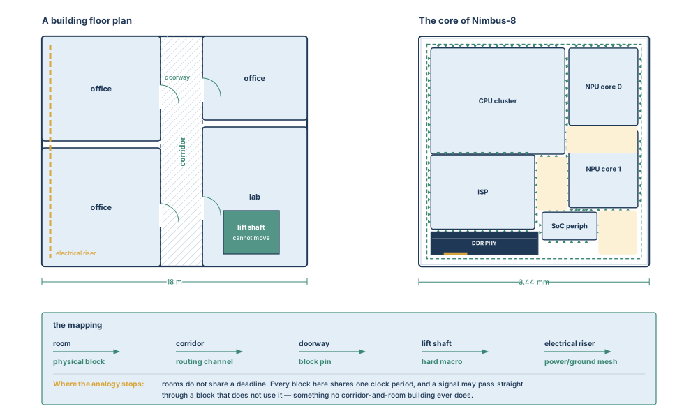
Two rooms in a building are independent once the walls are up. Two blocks on a chip are not. They share one clock period, so if one block is slow the other must be faster, and somebody has to decide by how much before either team starts work. And a signal on a chip may need to enter one block and leave the other side without being used inside it at all — a feedthrough, which has no architectural equivalent. Every time this book says “think of it as a room”, remember these two exceptions.
Now the engineering model
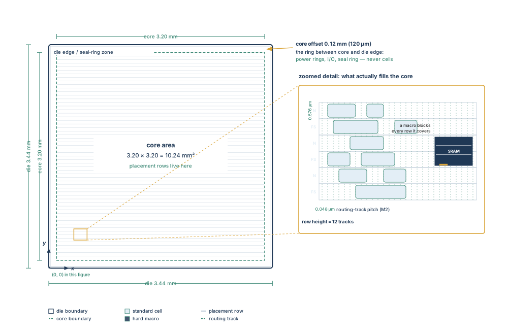
Strip the analogy away and the model is concrete. A chip is fabricated as a rectangle of silicon called the die. Inside the die, set back from its edge, is the core: the region where logic cells are allowed to sit. The strip between core and die edge — the core offset — is not wasted either; it carries power rings, input/output structures and the seal ring that protects the die when it is cut from the wafer. No standard cells go there.
The core is not smooth. It is ruled into placement rows, each exactly as tall as the standard cells in your library, because a standard cell may only sit on a row, aligned to it, the way a book sits on a shelf. Crossing the rows, in every metal layer above, are routing tracks: the evenly pitched lines that wires are expected to follow. Rows tell you how much logic fits. Tracks tell you how much wiring fits. A floorplan that ignores either one will fail late and expensively.
Two kinds of things get placed in the core. A standard cell is a small library cell — an inverter, a flip-flop — one row tall, and there are millions of them. A hard macro is a large pre-built object such as a static random-access memory (SRAM) or a physical interface block: it arrives fully designed, it cannot be reshaped, it is taller than a row, and it blocks the rows it covers. You place macros. You do not synthesise them.
Do not confuse these
| This | Not this | How to tell them apart in one question |
|---|---|---|
| Die | Core | Does it include the ring that holds power rings, I/O and the seal ring? Then it is the die. The core is only the cell-legal region inside it. |
| Logical hierarchy | Physical hierarchy | Did a human write it in RTL, or did you choose it as a planning boundary? Modules are logical; blocks are physical and exist only after you commit them. |
| Module | Block | Can it be planned, shaped and handed to a team on its own? Then it is a block. Until then it is a module inside its parent. |
| Standard cell | Hard macro | Is it one row tall and reshapeable by the tools? Standard cell. Fixed size, blocks rows, arrives pre-built? Hard macro. |
| Signal routing | Power and ground routing | Does the wire carry information or current? PG wiring is planned as a pattern of rings, meshes and rails; signal wiring is planned as topology and budgets. |
| Utilisation | Congestion | Utilisation is an area ratio you can compute by hand. Congestion is a wiring-demand result you must ask a router for. High utilisation makes congestion likely; it does not measure it. |
| Abstract | Full block | Does it contain the whole netlist, or only what the current task needs — boundary, pins, blockages, timing? The reduced view is the abstract. |
| Estimate | Signoff result | Was it produced from a plan with no real clock tree and no real routes? Then it is an estimate, and it is allowed to be wrong. Say so when you report it. |
| Block boundary | Block origin | The boundary is the outline the block occupies; the origin is the coordinate reference its internal objects are measured from. Both can be changed, and confusing them moves everything by a constant. |
1.2 The concepts, built in dependency order
The rest of this chapter builds the subject one idea at a time, in the order the ideas depend on each other. Read the subsections in sequence the first time. Afterwards, each one is short enough to be re-read on its own.
1.2.1 What design planning is for
Design planning is an integral part of the path from register-transfer level (RTL) description to the final layout data. It exists for two reasons.
The first is feasibility. You want to know early — while changes are still cheap — whether a given implementation strategy can work. Is this die big enough? Can these blocks be placed so that the critical paths stay short? Will the wires fit? A planning run answers those questions in hours, using estimates, instead of finding the answer weeks later using a full implementation.
The second is divide and conquer. A design with millions of cells is expensive to process as one flat object. Splitting it into smaller, more manageable pieces lets separate teams work on separate blocks in parallel, from RTL all the way through physical implementation, and lets the tools work on one piece at a time. Working with smaller blocks — and reusing one block in several places — reduces overall runtime.
Why not just implement the whole chip flat and skip planning? For a small design you sometimes can, and the tool supports flat flows. But three things push large designs towards a planned hierarchy: the design may need excessive computing resources to process flat; some blocks may arrive late and you need a methodology that absorbs late changes to one block without disturbing the schedule of the others; and the design may contain hard intellectual-property macros such as RAMs, or a block that was implemented before and can be converted and reused. If any of those is true of your project, a hierarchical plan is not a luxury.
1.2.2 What floorplanning actually is
Floorplanning is the concrete work inside design planning. It means: partitioning logical modules into physical blocks; sizing and placing those blocks; performing a floorplan-level placement of macros and standard cells; and creating a power plan. The purpose is to make every downstream physical step more efficient, so that the design can be optimised robustly rather than rescued repeatedly.
An effective floorplan helps timing close, because placing blocks well makes critical paths short and reduces routing congestion. The difficulty is that the two goals fight each other. You want a small, area-efficient footprint, because area is money. You also want enough space left for routing, because wires need room. A floorplan that is too generous wastes silicon on every chip ever shipped. A floorplan that is too tight cannot be routed, and you will discover that after weeks of work.
Floorplanning is also iterative by nature. A realistic sequence reshapes the blocks, creates a new cell placement, reallocates the timing budgets, re-checks top-level timing, and goes round again until the floorplan is good enough. Expect several passes. An engineer who describes the first floorplan as “done” has not yet measured it.
…you add 10 % to the die instead of improving the plan? Every wafer costs the same to process, so cost per good die rises with area; yield falls as die area grows; and the longer wires that come with a bigger floorplan cost delay and switching power. The plan usually has more slack in it than the die does — which is why enlarging the die is the last lever a senior engineer reaches for, not the first.
1.2.3 Area arithmetic: the calculation you must be able to do by hand
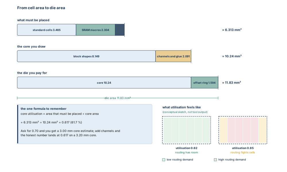
Everything physical starts from one ratio. Core utilisation is the total area occupied by all standard cells and macro cells divided by the total core area. It is expressed as a number between 0 and 1: a core utilisation of 0.80 means 80 % of the core area is used for cell placement at this stage, and the remaining area is available for routing and for the cells that later steps will add.
That definition is worth reading twice, because two details in it catch people out. First, macros count: a design that is 30 % SRAM by area has far less standard-cell freedom than its cell count suggests. Second, it describes the area at this stage. Optimisation, clock-tree synthesis and hold fixing all add cells later, so a plan that starts at the utilisation you can just barely route has already failed.
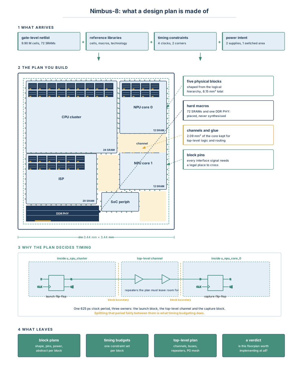
Here is the arithmetic for this book’s teaching design, Nimbus-8, a small edge-inference system-on-chip. Every number in the table below is used again in later chapters, so it is worth following the calculation rather than skimming it.
| Quantity | symbol | Calculation | Value |
|---|---|---|---|
| Standard cells to place | N | from the netlist | 9.90 M |
| Average standard-cell area | a | library average for this design mix | 0.350 µm² |
| Standard-cell area | A_std | 9.90 × 10⁶ × 0.350 µm² | 3.465 mm² |
| SRAM macros | — | 72 instances × 0.0320 mm² | 2.304 mm² |
| DDR PHY macro | — | one hard IP instance | 0.544 mm² |
| Area that must be placed | A_place | 3.465 + 2.304 + 0.544 | 6.313 mm² |
| First core estimate at 0.70 | A_core | 6.313 ÷ 0.70 | 9.019 mm² → 3.003 mm square |
| Core chosen after channel allowance | — | 3.20 mm × 3.20 mm | 10.24 mm² |
| Resulting core utilisation | U | 6.313 ÷ 10.24 | 0.617 |
| Die with 0.12 mm core offset | — | (3.20 + 2 × 0.12)² | 3.44 mm × 3.44 mm = 11.83 mm² |
Notice what happened between the two core numbers. Asking for a utilisation of 0.70 produces a 3.00 mm core — but that number quietly assumes the whole core can be filled with blocks. In a design with top-level logic sitting between the blocks, it cannot: some of the core must stay as channel. Once 2.09 mm² of channel is reserved, the honest core is 3.20 mm square and the honest utilisation is 0.617. Both numbers are correct; only one of them is a plan.
Write the area calculation into a text file with its assumptions — cell count, average cell area, macro list, target utilisation, channel allowance — and keep it beside the scripts. When someone asks in month four why the die is 3.44 mm, that file is the answer. Without it, the honest answer is “because it was 3.44 mm in month one”, which is how chips end up larger than they need to be.
1.2.4 Logical hierarchy, physical hierarchy, and the moment one becomes the other
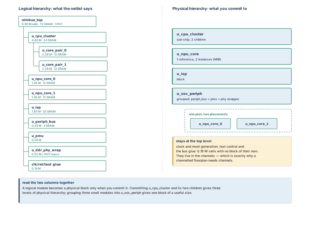
A netlist has a logical hierarchy: modules inside modules, written by designers for reasons of readability, reuse and verification. It has no physical meaning at all. Nothing about a module says where it sits, how big it is, or what shape it takes.
A physical hierarchy is something you choose. You select certain logical modules and declare that each will be planned, shaped, placed, routed and handed over as a unit. That declaration is called committing the module, and the result is a physical block. Blocks are committed early in the floorplanning flow, precisely so that the reduced views built from them can be used to produce an initial floorplan and initial timing budgets.
What changes in the database when you commit? The module stops being merely a name inside its parent and becomes an object with a boundary, an origin, pins where its nets cross that boundary, its own area target, and its own constraints. It can then be opened separately, planned separately, and given to another engineer. That is a genuine change of kind, not a label.
Two aids exist for the decision itself. A hierarchy browser in the graphical interface lets you navigate the design hierarchy, examine the logical structure, and read per-module information such as utilisation, standard-cell count and pin count — which is exactly the data the decision needs. For the same information in text form, ask the tool for a hierarchy report. Then, once you have decided, you commit.
1.2.5 Floorplan style: channelled or abutted
The tool supports complete hierarchical planning for both layout styles, and the choice interacts directly with your partitioning.
In an abutted floorplan the blocks sit directly against one another and there is no top-level logic between them. In a channelled floorplan there are gaps between blocks, and those gaps hold top-level logic — either a small amount or a large amount. There is also a narrow-channel variant for the case where the gaps are deliberately thin.
The consequence is simple and often missed by beginners: if your partition leaves cells at the top level, you cannot have an abutted floorplan, because those cells have nowhere to sit. Nimbus-8 keeps 0.19 M cells of clock generation, reset synchronisation and test control at the top, so Nimbus-8 is a channelled design, and 2.09 mm² of its core is reserved accordingly. Had we pushed every one of those cells down into blocks, an abutted style would have become possible — and the design would have had a smaller core but stiffer block interfaces.
1.2.6 Deciding where the boundaries go
Partitioning is the highest-leverage decision in the whole planning stage, and it is made with judgement informed by four factors.
| Factor | What it asks | What you do about it |
|---|---|---|
| Size | Are the blocks of similar size? | Group small modules together; divide large ones when it is appropriate to do so. |
| Function | Does the cut follow the functional units your verification and simulation people work with? | Partition along functional units, and watch top-level connectivity and block pin counts to avoid congestion and timing problems. |
| Floorplan style | Does the physical hierarchy support the style you intend? | Different styles need different hierarchies: abutted has no top-level logic, channelled has a small or large amount. |
| Common hierarchy with synthesis | Does the physical hierarchy match the one used in the synthesis tool’s topographical mode? | Keep them the same, so that scan-chain description data can be exchanged between block level and top level. |
Read those four in order and a rhythm appears: get the sizes comparable, respect function, match the style, align with synthesis. Figure 1.7 turns the same four factors into something you can walk through module by module.
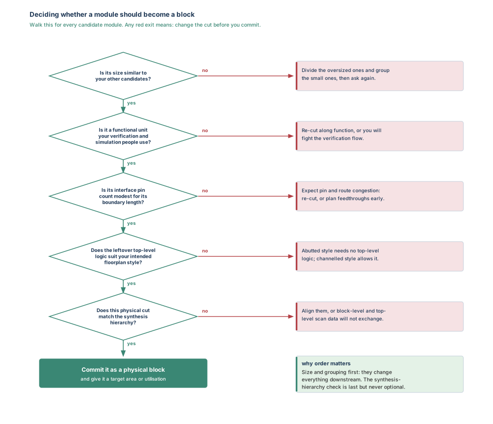
…you commit five small blocks instead of grouping them into one? Each block brings a boundary, a pin set, an abstract view, a timing budget, a set of checks and a person who owns it. Five of those for 0.36 M cells is a poor trade: the pins alone can cost more routing resource than the logic saves. This is why grouping is listed as a factor in its own right rather than as an afterthought.
1.2.7 More than two levels of hierarchy
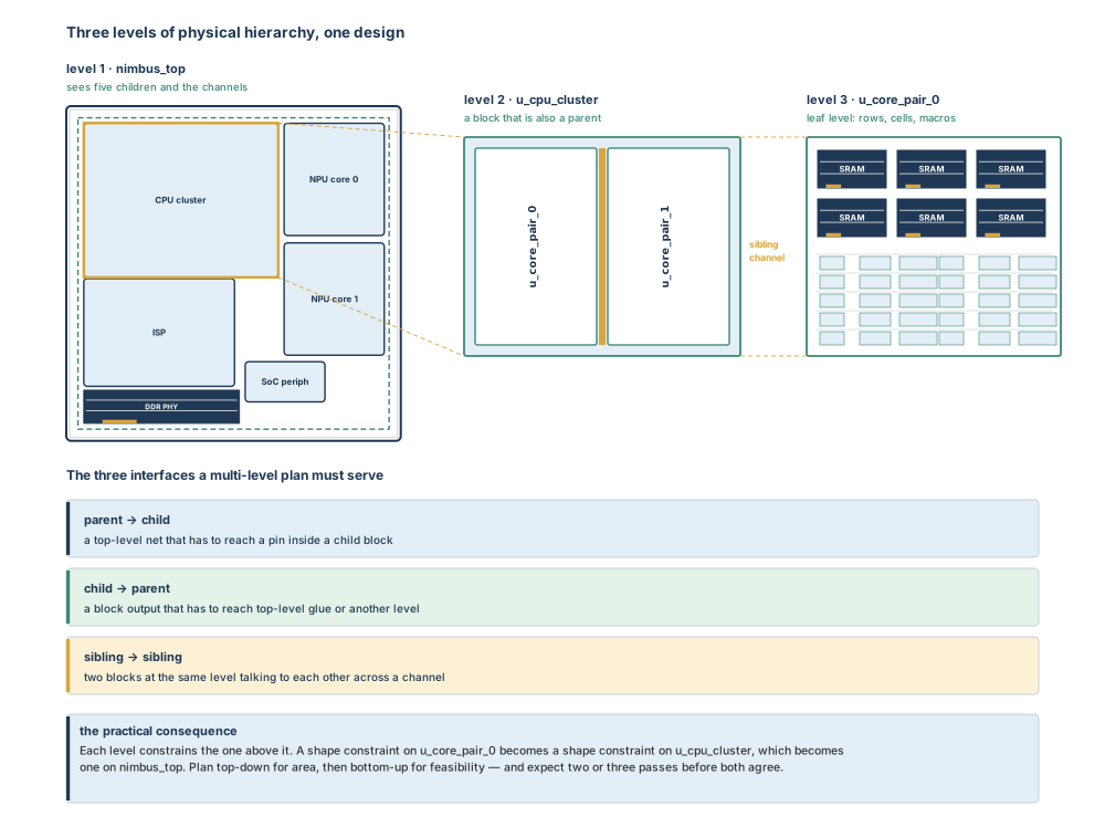
Many tools are limited to two levels of physical hierarchy — top and block. Large system-on-chip designs frequently need more, and the tool provides comprehensive support for multiple levels at the same time, which is what makes it possible to treat u_cpu_cluster as a block that is itself a parent. You can enable or disable specific blocks and levels of hierarchy for planning with the set_editability command, which is how you keep a large multi-level design manageable while working on one part of it.
Support for extra levels is not a single feature; it appears in every planning function, and it is worth knowing where:
- Data model. Multiple levels of physical hierarchy are built into the data model, so shaping, placement, routing and timing can each reach the specific data they need for a given level quickly.
- Block shaping. The shaper needs each sub-chip’s target area, the aspect-ratio constraints imposed by hard macro children, and the interconnect that exists at sibling-to-sibling, parent-to-child and child-to-parent interfaces — plus, in multivoltage designs, the target locations of voltage areas. Shaping constraints on lower-level sub-chips are propagated upward as shaping constraints on their parents. Notably, the shaper does not need the full netlist inside each block, which is what keeps it fast.
- Cell and macro placement. After shaping, placement sees a global view of interconnect paths and data flow at the hierarchy boundaries, so it can place macros for every sub-chip at every level, reserve resource at adjacent sub-chip edges for the paths that must cross, and avoid positions where a path would need heavy buffering to get across a macro. It models the environment outside each sub-chip’s boundary, then distributes the per-sub-chip placement jobs across processes to shorten turnaround.
- Power planning. Construction rules — widths, layers, pitches — are described as reusable patterns and applied to regions such as voltage areas or macro groups, with strategies binding patterns to regions. From your top-level specification the tool characterises the plan and generates strategy definitions for sub-chips at all levels, so a floorplan change at any level can be followed by regenerating the power plan instead of redrawing it.
- Pin placement. With shapes formed, macros placed and power routed, pin placement gathers interface data from all levels and calls the global router to find good pin locations, aligning pins across levels where it can. It also creates the feedthroughs that let a signal cross a block it does not use, decides where a feedthrough can be reused, and connects unused ones to power or ground as required.
- Timing budgeting. The tool estimates timing at the hierarchical interfaces and creates budgets for the sub-chips: constraints for child interface pins in the full chip, for parent and child interfaces of mid-level sub-chips, and for the primary pins of the lowest-level sub-chips. With those in hand, the whole design can proceed into placement and optimisation concurrently.
You can also view, analyse and edit any level in full-chip context, choosing to see the top level alone or several levels at once. When several levels are shown, interactive routing behaves as though the design were flat; when you finish, the routes are pushed into the children and the hierarchical pins are added automatically.
1.2.8 One block, many placements: multiply instantiated blocks and feedthroughs
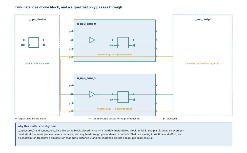
When the same block appears more than once in a design it is a multiply instantiated block, universally abbreviated MIB. Nimbus-8 has one: a single NPU (neural processing unit) core reference placed twice. You plan it once and place it twice, which is one of the strongest runtime and effort savings available in a hierarchical flow.
The saving comes with a constraint that beginners consistently underestimate. Because every instance is the same block, the pin placement must work for all of them: the algorithm determines a placement that suits every instance and makes the pin positions identical on each. A pin location that is ideal for instance 0 and awkward for instance 1 is not a legal location at all. The same applies to feedthroughs — the global router creates them across MIBs, decides which can be reused, and ties unused ones off to power or ground.
A feedthrough is a path provided through a block for a signal the block does not use. Without it, a net that needs to get from one side of the die to the other must detour around every block in the way, which costs wire length, delay and routing resource in the channels — often exactly where they are scarcest.
1.2.9 Sharing the clock period: timing budgets
Here is the idea that makes hierarchical planning possible at all. Two blocks that exchange a signal cannot be optimised independently unless somebody first decides how much of the clock period each of them is allowed to consume. That decision is a timing budget.
The tool estimates timing at the hierarchical interfaces and creates budgets for the sub-chips, so that each block team receives ordinary timing constraints describing its own slice and can then work alone. Figure 1.10 shows what the arithmetic looks like for one path in Nimbus-8: a 625 ps clock period, minus the clock uncertainty and the capture flip-flop’s setup requirement, leaves 550 ps to be divided between the launching block, the top-level channel and the capturing block.
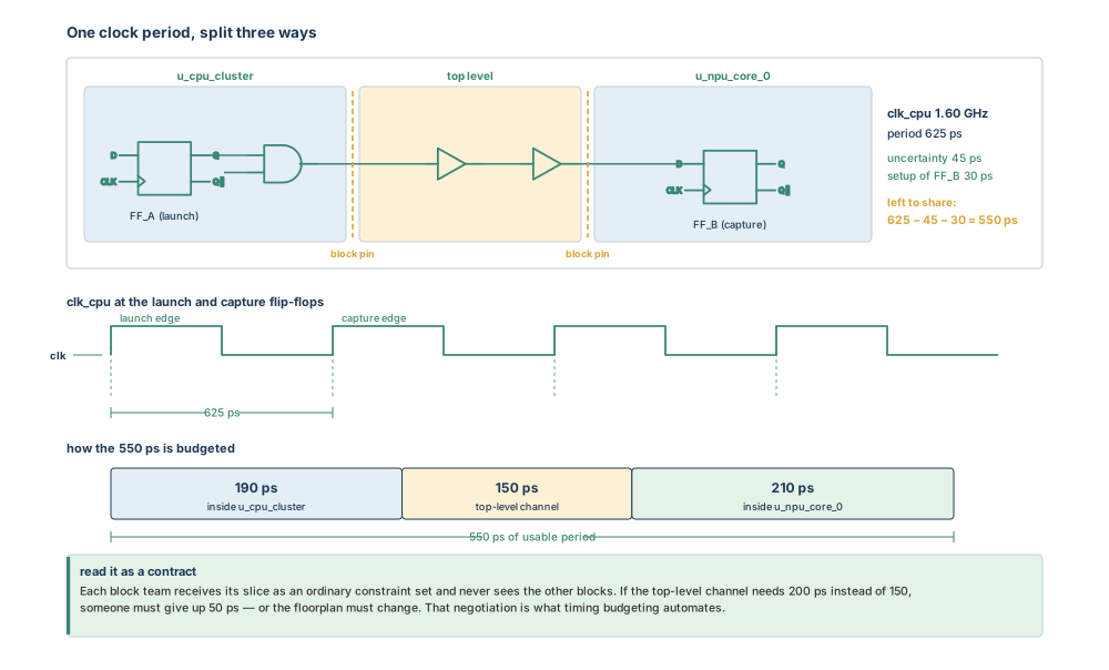
Budgets are built from estimated interconnect, with no real clock tree and no real routing. They are an educated forecast, not a signoff result, and they will be revised. Reporting an estimate as though it were signoff timing is one of the fastest ways for a junior engineer to lose credibility; saying “this is a planning estimate, and here is the assumption behind it” is one of the fastest ways to earn it.
1.2.10 The shape of the flow
You now have every concept needed to read the flow itself. Design planning is performed during the first stage of the hierarchical flow, after the initial netlist is available from synthesis, and it does three things: it partitions the design into blocks, it generates hierarchical physical constraints, and it allocates top-level timing budgets down to the physical blocks.
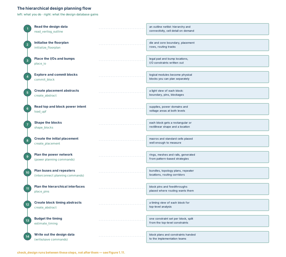
Figure 1.5 lays the whole sequence out with the command that drives each step and — just as important for a beginner — what the design database has gained by the time the step is finished. Do not try to memorise it. Read it as a map, and notice three things about its shape.
First, the physical comes before the temporal: shapes, macros, power and pins are settled before timing is budgeted, because the budget depends on distances that do not exist until the shapes do. Second, abstracts appear twice, once for placement and once for timing, because the two tasks need different reduced views of the same block. Third, the sequence is a loop, not a line: a bad budget sends you back to the floorplan, and the last step of a first pass is usually the first step of a second one.
1.3 Inputs, outputs and readiness
What has to exist before planning starts
| Input | Why planning needs it | Consequence if it is wrong or missing |
|---|---|---|
| Gate-level netlist from synthesis | The list of cells, macros and nets to be divided and placed. Planning reads it as an outline view, which keeps the hierarchy and connectivity available while deferring cell-level detail until it is needed. | No cell counts, so no honest area budget; a netlist from a different RTL revision silently plans the wrong chip. |
| Reference and technology data | Cell and macro geometry, layer definitions, preferred routing directions and site definitions — the source of row height, track pitch and legal placement. | Layer directions or tracks missing, and the floorplan cannot be initialised meaningfully. |
| Timing constraints | Clocks, their periods and the operating conditions to analyse. Budgeting cannot divide a period it has not been told about. | Unconstrained endpoints, meaningless budgets, and a plan optimised for a clock nobody will use. |
| Power intent | Supplies, power domains and voltage areas, at the top level and at block level. Shaping and power planning both consume it. | Voltage areas cannot be shaped or powered correctly; multivoltage checks fail late. |
| Per-block file mapping | Which constraint file and which power-intent file belong to which block. The abstract-creation steps expect this mapping to be complete. | A block with no listed constraint or power file blocks abstract creation for the whole design. |
| Area or utilisation target per block | What the shaper sizes each block from. | Shaping fails or produces nonsense — the single most common beginner error in this stage. |
| Advanced-node floorplan rules (if applicable) | Node-specific spacing, enclosure, halo, width, density and area rules that a modern floorplan must satisfy. | A floorplan that looks fine and violates the technology. |
Assumptions you are making, whether you say so or not
- That the average cell area you used is representative of this design, not of the last one.
- That the macro list is complete — including the macros that arrive in month three.
- That a black-box module (Chapter 5) will eventually fit in the area you typed for it — that area is spent, not a placeholder.
- That the clocks in the constraint file are the clocks the architects intend to ship.
- That your physical hierarchy matches the one synthesis used, if you intend to exchange scan-chain data.
Write each of these down with its value. An assumption on paper is a decision; an assumption in your head is a future argument.
Preflight checklist
- Netlist revision recorded, and it matches the constraint revision.
- Technology data loaded; layer directions set; both horizontal and vertical routing layers present.
- Cell count and macro inventory extracted, and the area budget computed and saved with its assumptions.
- Target utilisation and channel allowance chosen deliberately, and written down.
- Candidate partition listed module by module, with each module’s cell count, macro count and pin count.
- Floorplan style decided, and consistent with the amount of logic left at the top level.
- Per-block constraint and power-intent files listed for every block you intend to commit.
- The pre-floorplan validation gate run and clean.
What you get out
Planning changes the design database, and it is worth being precise about what appears in it. After a full pass you have: a die and core boundary with placement rows and routing tracks; committed blocks with boundaries, origins and pins; reduced views of each block for placement and for timing; block shapes and locations; an initial macro and cell placement; a power plan generated from patterns and strategies; planned buses, repeaters and routing corridors; placed hierarchical pins and the feedthroughs that go with them; one timing-constraint set per block; and written-out data for the implementation teams.
You also get something that is not a file: a defensible answer to the question “can this be built?”. That answer is the real deliverable.
When planning is premature, unsafe or misleading
| Condition | Why it matters |
|---|---|
| The netlist is not from a settled RTL revision | Cell counts move, and every area number moves with them. Plan anyway if you must, but label the result as exploratory. |
| Major macros are still unknown | Macro area dominates the budget. A missing 0.5 mm² memory is 5 % of this chip’s core. |
| No target area or utilisation for one or more blocks | Shaping has nothing to work from, and the failure often looks like an unrelated overlap error. |
| Layer directions or tracks not set | Rows and tracks define what “fits”. Without them, area feedback is fiction. |
| Constraints have unconstrained clocks or missing corners | Budgets cannot be produced for what has not been constrained, and the ones you do get will be optimistic. |
| The physical hierarchy disagrees with synthesis | Legal, and it will plan — but scan data will not exchange between levels, and you will find out much later. |
| Results are being reported as signoff quality | They are estimates. Presenting them otherwise causes decisions that cannot be justified when real timing arrives. |
1.4 The guided workflow
This section walks the flow end to end at survey level, then treats in detail the four commands that belong to this chapter. The deeper commands are named here so that you can see where they fit, and taught properly in the chapter that owns them — a command is best learned once, in context, not twice in outline.
1.4.1 The fourteen steps, and where each is taught
| # | Step | Command | Taught in |
|---|---|---|---|
| 1 | Read the design data | read_verilog_outline | Chapter 4 |
| 2 | Initialise the floorplan | initialize_floorplan | Chapter 4 |
| 3 | Place the I/Os and bumps | place_io | Chapter 6 |
| 4 | Explore the hierarchy and commit blocks | explore_logic_hierarchy, commit_block | Chapter 8 |
| 5 | Create block placement abstracts | create_abstract | Chapter 8 |
| 6 | Read top- and block-level power intent | load_upf | Chapters 3 and 10 |
| 7 | Shape the blocks | shape_blocks | Chapter 9 |
| 8 | Create the initial placement | create_placement | Chapter 9 |
| 9 | Plan the power network | power-planning commands | Chapter 10 |
| 10 | Plan buses and repeaters | interconnect-planning commands | Chapter 11 |
| 11 | Plan the hierarchical interfaces | place_pins | Chapter 13 |
| 12 | Create block timing abstracts | create_abstract | Chapter 14 |
| 13 | Budget the timing | estimate_timing | Chapter 14 |
| 14 | Write out the design data | write and save commands | Chapters 4 and 8 |
Three topics sit alongside the main line rather than inside it: blocks whose contents do not exist yet (Chapter 5), designs stacked in three dimensions (Chapter 7), and the planning of clock distribution across blocks (Chapter 12). The interface conventions, scripting and monitoring that make all of this comfortable to drive are Chapter 2.
1.4.2 Validation: the gate before every step
Design planning has a checking command, and the single most useful habit you can form in this chapter is to run it before a step rather than after it. You specify the command with the -checks option followed by one or more check keywords, and the tool performs those checks on the current design:
icc2_shell> check_design -checks {dp_pre_floorplan}
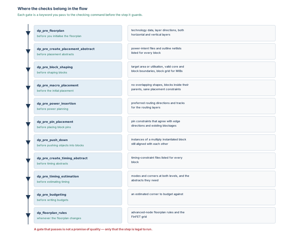
Each planning keyword guards a particular step. Table 1.7 lists them with what they examine, and Figure 1.11 shows the same information positioned along the flow.
| Keyword | What it checks |
|---|---|
| dp_pre_floorplan | That the technology file information is correct, that layer directions are set, and that the design contains both horizontal and vertical layers. |
| dp_pre_create_placement_abstract | That the constraint mapping specifies a power-intent file for all blocks, and that the outline-view netlist files are in place for the blocks. |
| dp_pre_block_shaping | That a target utilisation or area exists for all black boxes; that there is at least one block or voltage area to shape; that the core area and block boundaries are valid; that the block grid is set if the design contains multiply instantiated blocks; and the multivoltage checks related to shaping. |
| dp_pre_macro_placement | That block shapes do not overlap; that blocks and voltage areas lie inside their parent boundaries; basic placement-constraint checking such as overlapping or out-of-bounds relative-location constraints, macro width and height against the FinFET grid, and macro orientation; that each block has a logical hierarchy; block, voltage-area and movebound utilisation; and the multivoltage checks related to placement. |
| dp_pre_power_insertion | That the preferred routing direction is set for the routing layers, and that tracks exist for the routing layers. |
| dp_pre_pin_placement | Pin-constraint checks — topological constraints, individual constraints, constraints propagated from individual pins, bundle and block pin constraints, size-related constraints, pin guide and pin blockage constraints, routing guide and routing blockage constraints; that each layer’s routing direction in a topological constraint is consistent with the block edge constraints; consistent edge directions in topological constraint pairs; off-edge pins that are part of a feedthrough constraint; possible overlaps with existing internal block objects such as route blockages, pin blockages, fixed pins and prerouting; plus the multiply-instantiated-block pin-placement checks. |
| dp_pre_push_down | The alignment checks for multiply instantiated blocks. |
| dp_pre_create_timing_abstract | That the constraint mapping specifies timing-constraint files for all blocks. |
| dp_pre_timing_estimation | That top and block levels have defined modes and corners; that top-level modes and corners have corresponding block-level ones; and that the top level contains at least one clock, at least one scenario using a non-estimated corner, and a corner with parasitic parameters. With placement abstracts present, it also confirms that the abstracts exist. |
| dp_pre_budgeting | That the estimated corner is available, plus the same checks as timing estimation. |
| dp_floorplan_rules | The segment parity rule, the macro spacing rule, and the FinFET grid checks. |
1.4.3 A first session, step by step
The workflow below is the one this chapter can complete on its own: understand the design, decide the partition, and prove readiness. Steps that belong to later chapters are marked as such and deliberately not expanded.
- Open the design. Library setup, block opening and the shell itself are Chapter 2. For now, assume a session with the design open.
- Read the hierarchy. Produce a hierarchy report and, if you have the graphical interface, the hierarchy browser. Record for each candidate module: cell count, macro count, pin count.
- Compute the area budget by hand (Table 1.2). Do not skip this because the tool can report utilisation later; the point is that you know the number before the tool tells you.
- Decide the partition using Table 1.3 and Figure 1.7. Write the decision and its reasons in the script as comments.
- Decide the floorplan style and reserve channel area consistent with the top-level logic you are leaving behind.
- Scope your session with
set_editabilityif the design has several levels and you only intend to work on part of it. - Run the readiness gate for the step you are about to take — here,
dp_pre_floorplan. - Read the message summary, not just the last line. Fix the rules that were reported, and re-run until the gate is clean.
- Only then proceed to floorplan initialisation (Chapter 4).
1.4.4 Command reference for this chapter
Four commands are genuinely part of this chapter’s work. Each is presented the same way: what it is for, what its syntax says in plain English, what must be true before you use it, a small realistic example, what to expect, how to verify, what goes wrong, and how to see the rest of its options.
report_hierarchy — see the structure you are about to divide
Purpose. Displays the logical and physical reference hierarchy for a block, so you can see what modules exist, which are already physical blocks, and where the leaves are.
Syntax in plain English. report_hierarchy with no arguments reports on the current block, showing both physical and logical references down to leaf level. -block names a different block to report on. -physical_context restricts the report to physical blocks and leaf modules, hiding internal modules. -hierarchical unfolds repeated blocks or modules that would otherwise be reported once. -no_leaf leaves the leaf modules out. -nosplit stops long fields from being wrapped onto a second line, which matters if you intend to post-process the report with a script.
Prerequisites. A design open in the session.
# What does the hierarchy look like, without the leaf-cell noise?
icc2_shell> report_hierarchy -no_leaf

# Only the physical picture: blocks and leaf modules, no internal modules.
icc2_shell> report_hierarchy -physical_context -no_leaf

# Unfold repeated instances instead of folding them into one line.
icc2_shell> report_hierarchy -hierarchical -no_leaf
Expected result. An indented tree. Blocks are printed with their full name, which distinguishes them from internal modules; leaf modules are shown with the library they come from. Repeated blocks or modules are folded into a single appearance unless they are bound to different views, or unless you ask for the unfolded form.
Verification step. Compare the tree against the module list you were given by the front-end team. Two mismatches matter: a module you expected to see and cannot, and a module that appears with a different reference than you expected.
Common mistakes. Reading the folded report as though it showed instance counts — a block used twice appears once by default. Reporting the wrong block because the current block is not the one you think it is. Post-processing a report captured without -nosplit and losing half of the long names to line wrapping.
Finding the rest. report_hierarchy -help lists the options; man report_hierarchy gives the full description.
get_design_checks — find out which checks exist
Purpose. Creates a collection of the available checks, both the ones predefined by the tool and any you have defined yourself. Use it when you want to know what is available rather than guessing a keyword.
Syntax in plain English. get_design_checks with a pattern returns the checks whose names match it. -filter narrows the collection using a Boolean expression over check attributes; -regexp treats the pattern as a regular expression rather than a wildcard; -nocase ignores case; -exact turns pattern matching off, which is what you need when a name itself contains * or ?; -quiet suppresses the warning when nothing matches.
Prerequisites. A session with the tool loaded. You do not need a floorplan.
# Which planning checks does this version of the tool provide?
icc2_shell> get_design_checks dp_*

# Everything, when you want to browse the whole list once.
icc2_shell> get_design_checks

# Which attributes can I filter on?
icc2_shell> list_attributes -class ems_check
Expected result. A collection of check objects. Predefined checks are those the tool ships with; user-defined checks are ones created with the check-strategy command. Some predefined checks are single checks; others are collections of several, so running one keyword can run a group.
Verification step. Confirm that the keyword you are about to pass to the checking command appears in this list. That single step removes an entire class of confusing failures.
Common mistakes. Assuming a keyword that existed in one release exists in the next; typing a keyword from memory rather than from the list; and forgetting that names are patterns by default, so a stray wildcard can return more than you meant.
Finding the rest. get_design_checks -help, then man get_design_checks.
The set of available checks, and what each one examines, can change between tool releases. That is a good thing — checks get stronger — but it means a script that hard-codes a keyword can fail after an upgrade. Ask the tool which checks exist rather than trusting a list copied from an older project, including the list in Table 1.7.
check_design — prove the design is ready for the next step
Purpose. Runs predefined or user-defined checks on the current design. The messages produced are captured into a message database and a text log, and a summary of them is reported.
Syntax in plain English. -checks takes a list of one or more check names and is required. -ems_database names the database file the errors, warnings and information messages are stored in; if you do not give one, a default file name is used, and an existing file of that name is overwritten. -log_file names the text log to write; by default the tool generates one whose name carries a timestamp, in the working directory. -open_message_browser opens the graphical message browser on the results.
Prerequisites. The design open, and whatever data the specific check needs — technology data for the pre-floorplan check, blocks and targets for the shaping check, and so on. A check with nothing to inspect reports nothing useful.
# The gate before floorplan initialisation.
icc2_shell> check_design -checks {dp_pre_floorplan} \
               -log_file reports/ch01_pre_floorplan.log

# Two gates at once, into a named message database.
icc2_shell> check_design -checks {dp_pre_floorplan dp_floorplan_rules} \
               -ems_database reports/nimbus_pre_fp.ems \
               -log_file reports/nimbus_pre_fp.log
Expected result. A report header naming the command, the options you passed and the design, followed by the checks as they run and then a message summary: one line per rule, giving the rule identifier, its type — error, warning or information — the count, and the message text. A total line follows, and the message database is saved.
*** EMS Message summary ***
-----------------------------------------------------------------
Rule    Type  Count  Message
-----------------------------------------------------------------
...     Error   n    <one line per rule that fired>
...     Warn    n    <one line per rule that fired>
-----------------------------------------------------------------
Total N EMS messages : n errors, n warnings, n info.
Verification step. Two questions, in this order. Is the error count zero? And of the warnings, which ones are about the step you are about to run? A warning that names the very data the next command consumes is not a warning; it is an error that has not happened yet.
Common mistakes. Running it after a step instead of before. Reading only the total line — the rule identifiers are the actionable part. Letting the default database name overwrite the previous run’s evidence when you wanted to compare two runs. Passing a keyword that does not exist in your release. And treating a clean gate as proof of a good floorplan: it proves legality, not quality.
Finding the rest. check_design -help for the options, man check_design for the description, and get_design_checks for the keywords.
set_editability — decide which part of a big design you are working on
Purpose. Changes the hierarchical edit control of specified blocks, or their reference edit lock. In a design with several levels of physical hierarchy this is how you make one region editable for planning and leave the rest alone.
Syntax in plain English. -blocks lists the blocks whose editability changes, relative to the current top-level context; with no -blocks, the current block is affected. -value true makes them editable — the default — and -value false makes them uneditable. -from_level applies the value from a given design depth downward, and -to_level from a given depth upward; each of these is mutually exclusive with the other and with -blocks. -edit_reference_lock switches the meaning from hierarchical edit control to locking or unlocking the physical blocks for edit. -verbose prints more detail. The command returns the number of blocks whose control changed.
Prerequisites. A design with the blocks in question present in the current context.
# Work on the CPU cluster only; leave the rest of the design alone.
icc2_shell> set_editability -blocks {u_cpu_cluster} -value true -verbose

# Freeze everything from the second level of hierarchy downward.
icc2_shell> set_editability -from_level 2 -value false
Expected result. An integer count of the blocks that changed, and a design in which only the intended part can be edited.
Verification step. Attempt a harmless edit inside a block you intended to freeze and confirm that the tool refuses it, and one inside a block you intended to open and confirm that it succeeds. Two seconds of checking is cheaper than an afternoon of wondering why an edit did nothing.
Common mistakes. Combining -blocks with a level option — they are mutually exclusive. Forgetting that the default is true, so a call meant to freeze something opens it instead. Confusing hierarchical edit control with the reference edit lock: the first governs this top-level context, the second locks the block itself. And leaving a design frozen at the end of a session, so that the next engineer inherits a design that mysteriously refuses to change.
Finding the rest. set_editability -help, then man set_editability.
Three habits cover most of what this book cannot: help command for a one-line description, command -help for the list of supported options, and man command for the full page. Use them whenever a book — including this one — and your installed version disagree. The version in front of you is the one that is right.
1.5 Worked example: the first planning session on Nimbus-8
The situation
You have joined the physical design team for Nimbus-8, an edge-inference system-on-chip. Synthesis has produced a first gate-level netlist. The architects want to know two things by Friday: how big the die will be, and how the work will be divided between the four engineers on the team. Nobody has drawn a floorplan yet.
The inputs you have been given are the netlist, the reference and technology data for an advanced FinFET node, a constraint file with four clocks, and a power-intent description with two supplies and one switchable area. The DDR PHY is a hard macro that has already been characterised. There is no timing result of any kind yet, and there will not be one until a plan exists.
Initial conditions and assumptions
| Assumption | Value |
|---|---|
| Average standard-cell area for this design mix | 0.350 µm² |
| SRAM macro footprint (all 72 are the same compiled instance) | 0.0320 mm² |
| DDR PHY footprint | 0.544 mm² (1.60 mm × 0.34 mm) |
| Row height / routing-track pitch of the teaching library | 0.576 µm / 0.048 µm |
| Target block internal utilisation | 0.75 |
| Core offset for power rings and I/O structures | 0.12 mm per side |
| Clock to be budgeted first | clk_cpu, 1.60 GHz → 625 ps |
Step 1 — Read the hierarchy before touching anything
# What am I actually dealing with?
icc2_shell> report_hierarchy -no_leaf
From the report, and from per-module cell and macro counts, you build the inventory in Table 1.9. This table is the whole basis of the partition decision, so it is worth ten minutes of care.
| Module | Cells | SRAM | Cell area | Macro area | Needs at 0.75 |
|---|---|---|---|---|---|
| u_cpu_cluster | 4.60 M | 24 | 1.610 mm² | 0.768 mm² | 3.171 mm² |
| u_npu_core_0 | 1.45 M | 12 | 0.508 mm² | 0.384 mm² | 1.189 mm² |
| u_npu_core_1 | 1.45 M | 12 | 0.508 mm² | 0.384 mm² | 1.189 mm² |
| u_isp | 1.85 M | 20 | 0.648 mm² | 0.640 mm² | 1.717 mm² |
| u_periph_bus | 0.29 M | 4 | 0.102 mm² | 0.128 mm² | 0.306 mm² |
| u_pmu | 0.05 M | 0 | 0.018 mm² | — | 0.023 mm² |
| u_ddr_phy_wrap | 0.02 M | 0 | 0.007 mm² | 0.544 mm² | 0.553 mm² |
| clock/reset/test glue | 0.19 M | 0 | 0.067 mm² | — | stays at top |
| Total | 9.90 M | 72 | 3.465 mm² | 2.848 mm² | — |
Two facts jump out of that table. The CPU cluster is 2.7 times the size of the next largest candidate. And three modules — the peripheral bus, the power-management unit and the PHY wrapper — are each too small to justify their own block.
Step 2 — The first partition attempt, and why it is wrong
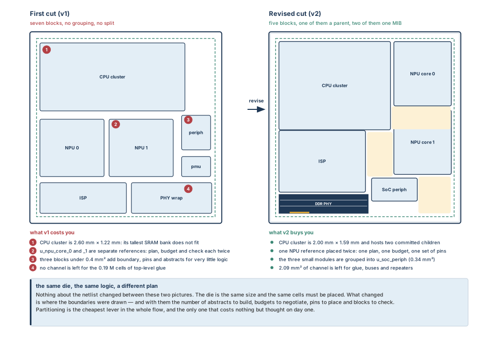
The obvious first cut is one block per top-level module: seven blocks, no thought required. Walk Figure 1.7 over it and it fails three of the five questions.
- Size. The CPU cluster is far larger than the others. To fit it beside two NPU cores and the ISP on a 3.20 mm core it has to be drawn long and thin — 2.60 mm × 1.22 mm — and its tallest SRAM bank no longer fits inside that height. The fix is to divide it: commit its two internal core pairs as blocks of their own, giving three levels of physical hierarchy.
- Size again, in the other direction. Three blocks under 0.4 mm² each bring three boundaries, three pin sets, three abstracts and three budgets. Group them into one block,
u_soc_periph, of 0.34 mm² — with the PHY itself left at the top level as a hard macro, since a wrapper containing one macro is not worth a block. - Repetition.
u_npu_core_0andu_npu_core_1are the same module. Committed as two separate references, they are planned twice, budgeted twice, checked twice and can drift apart. Committed as one reference with two instances — a multiply instantiated block — they are planned once.
Step 3 — Size the core from the revised partition
With the partition settled, redo the arithmetic in the order that matters: cells and macros first, then a first core estimate, then an honest core after channel allowance.
# Area that must be placed
A_std   = 9.90e6 x 0.350 um2            = 3.465 mm2
A_sram  = 72 x 0.0320 mm2               = 2.304 mm2
A_phy   = 1 x 0.544 mm2                 = 0.544 mm2
A_place                                 = 6.313 mm2

# First estimate: what would a 0.70 core look like?
A_core(0.70) = 6.313 / 0.70             = 9.019 mm2  -> 3.003 mm square

# Block shapes at 0.75 internal utilisation
cpu 3.171 + npu 1.189 x 2 + isp 1.717 + periph 0.339 + phy 0.544
                                        = 8.149 mm2

# A channelled style needs channel area for 0.19 M cells of glue,
# plus buses, repeaters and PG access. Choose 3.20 mm square:
A_core  = 3.20 x 3.20                   = 10.240 mm2
channel = 10.240 - 8.149                = 2.091 mm2   (20.4% of the core)
U_core  = 6.313 / 10.240                = 0.617

# Die, with 0.12 mm of core offset on each side
die     = (3.20 + 0.24) squared         = 3.44 x 3.44 mm = 11.83 mm2
Now you can answer the architects’ first question with a number and a reason: 3.44 mm square, because 6.313 mm² of cells and macros must be placed, 8.149 mm² of block shapes hold them at 0.75 internal utilisation, a channelled style needs about a fifth of the core as channel, and the core offset adds 0.12 mm on every side.
Step 4 — Prove readiness before initialising the floorplan
# Which planning checks exist in this release?
icc2_shell> get_design_checks dp_*

# Scope the session to the part of the hierarchy being planned.
icc2_shell> set_editability -blocks {u_cpu_cluster} -value true -verbose

# The gate that guards floorplan initialisation.
icc2_shell> check_design -checks {dp_pre_floorplan} \
               -log_file reports/nimbus_pre_fp.log
Suppose the summary comes back with a small number of errors and a larger number of warnings. Read it like this, in plain English:
| Type | What it means here | What you do |
|---|---|---|
| Error | The next step cannot run correctly on this data — for example, a routing layer with no preferred direction. | Fix it now. Errors from a pre-step gate are not advisory. |
| Warning | Something is unusual or incomplete. Some warnings are irrelevant to the step you are about to take; others name exactly the data it will consume. | Triage by relevance to the next command, not by count. |
| Info | A statement about the design, such as a structure not being present. | Read once. Keep the log; these lines are useful evidence later. |
Errors stop you. Warnings ask for judgement. But the most dangerous planning result is the one that produces no messages at all and a poor plan: a legal floorplan with a block shaped 3:1, or a core at 0.617 utilisation with all the slack in the wrong corner. No gate will complain. Only measurement and a second opinion catch it — which is what the engineering-judgement step below is for.
Step 5 — What a senior engineer looks at next
With a clean gate and a defensible die size, the plan is not finished; it is ready to be criticised. These are the questions a senior engineer asks, in this order, and each of them is the subject of a later chapter:
- Are the block aspect ratios sane? The CPU cluster at 2.00 mm × 1.59 mm is fine; at 2.60 mm × 1.22 mm it was not, because its tallest macro bank did not fit. Macro-driven shape constraints are Chapter 9.
- Is the channel where the traffic is? 2.09 mm² of channel is worthless if it sits in the corner while the buses run across the middle. Bus and repeater planning is Chapter 11.
- Can the pins get out? Count the interface signals per block and compare with the boundary length available at your usable layers. Pin and feedthrough planning is Chapter 13.
- Does the MIB constrain anything unacceptably? Both NPU instances share one pin plan; if their neighbours differ, one instance will have a longer route. Chapter 13 again.
- Where will the clocks cross? Four clocks and two blocks that share one of them means clock distribution must be planned across boundaries, not per block. That is Chapter 12.
- Is the budget survivable? 190 / 150 / 210 ps looks balanced; whether the 150 ps channel share is realistic depends on the distance between the two block pins, which the floorplan has just fixed. Budgeting is Chapter 14.
- What happens when the DDR PHY grows? Hard IP changes late. Ask now which direction it can grow in without redrawing the plan.
1.6 Failure modes and debugging
Every entry below follows the same five-part shape: symptom, likely cause, diagnostic check, correction, prevention. Read them once now and again after your first real planning session, when at least three of them will have happened to you.
| Symptom | Likely cause | Diagnostic check | Correction | Prevention |
|---|---|---|---|---|
| Block shaping fails; blocks overlap or fall outside the parent boundary | A block has neither a target area nor a target utilisation, so the shaper has nothing to size it from | Run the shaping gate and read the rule identifiers; confirm every block, including black boxes, has a target | Give every block a target area or utilisation, then re-run the gate before re-running shaping | Treat “every block has a target” as part of committing a block, not as a later step |
| Two instances of the same block end up misaligned | No block grid was set for a design containing multiply instantiated blocks | The shaping gate checks for a block grid when MIBs are present; the push-down gate checks alignment | Set the block grid, re-shape, and re-check alignment before pushing anything down | Identify MIBs during partitioning — before shaping, not after |
| Floorplan initialisation produces rows but no usable tracks | Layer directions not set, or the design lacks both horizontal and vertical layers | The pre-floorplan gate reports exactly this; also inspect the technology data | Fix the technology setup, then re-initialise the floorplan | Make the pre-floorplan gate the first command of every planning script |
| Area feedback looks wonderful and is wrong | Macros were omitted from the area budget, or an average cell area from a different design was reused | Recompute by hand: cell count × average area + macro area; compare with the reported utilisation | Rebuild the budget with the real macro inventory and re-size the core | Keep the area calculation and its assumptions in a file next to the scripts |
| Abstract creation stops before it starts | The per-block file mapping does not name a power-intent file, or an outline netlist, for some block | The pre-abstract gate names the blocks with missing files | Complete the mapping for every block, then re-run | Generate the mapping from the block list programmatically so it cannot go stale |
| Budgeting produces nothing, or produces budgets nobody can meet | Modes and corners are missing at one level, or the top level has no clock, no non-estimated corner, or no parasitic data | Run the timing-estimation and budgeting gates; they check precisely these conditions | Complete the mode, corner and scenario setup at both levels and re-run | Set up modes and corners before the first budgeting attempt, not in response to its failure |
| An edit appears to do nothing | The block is not editable in the current context, or its reference is edit-locked | Re-issue the editability command with verbose output and read the count of blocks changed | Open the intended scope, make the edit, and restore the scope afterwards | Set editability explicitly at the top of a script and reset it at the end |
| Scan-chain data will not exchange between block and top level | The physical hierarchy does not match the hierarchy used in synthesis | Compare the committed block list against the synthesis hierarchy, module by module | Align the two hierarchies — which usually means changing the physical partition | Agree the hierarchy with the synthesis owner before committing any block |
| Everything is legal and the plan is still bad | Legality is not quality: extreme aspect ratios, channels in the wrong place, pins on the wrong edge | Measure: aspect ratio per block, channel area versus where the buses run, pin count versus boundary length | Change the plan, not the die; re-shape and re-place, then compare against the previous pass | Add “what would I criticise if this were someone else’s plan?” to your own review |
| Advanced-node rule violations appear after a small floorplan edit | Node-specific floorplan rules and grid alignment were satisfied before the edit and not re-checked after it | Re-run the floorplan-rules gate after every floorplan change, however small | Repair the reported violations and re-check | Bind the rules gate to the end of any script that edits the floorplan |
The misleading one, in detail
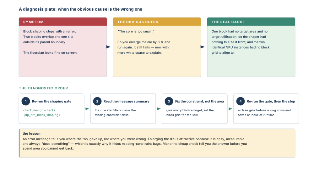
The first row of Table 1.11 deserves its own walkthrough, because its apparent cause and its real cause point in opposite directions. Shaping fails. Two blocks overlap, one sits outside its parent, and the floorplan looks perfectly reasonable on screen. The obvious reading is that the core is too small — so you enlarge the die by 8 % and run again. It fails again, and now you also have more white space to justify.
The real cause is that one block had no target area and no target utilisation, so the shaper had nothing to size it from, and the two identical NPU instances had no block grid to align to. Neither of those is an area problem. Both are named directly by the shaping gate, in seconds, if you run it.
1.7 Hands-on mini lab
Goal
Produce a defensible die size and a justified partition for a small synthetic design, and prove that the design is ready for floorplan initialisation. No proprietary data and no completed floorplan are needed; the arithmetic is the lab.
Supplied assumptions
| Module | Cells | SRAM macros | Interface signals |
|---|---|---|---|
| u_dsp_core_0 | 0.90 M | 8 | 420 |
| u_dsp_core_1 | 0.90 M | 8 | 420 |
| u_codec | 2.60 M | 16 | 610 |
| u_io_bridge | 0.18 M | 2 | 240 |
| u_rtc | 0.02 M | 0 | 40 |
| clock/reset glue | 0.10 M | 0 | — |
Average standard-cell area 0.350 µm²; SRAM macro 0.0320 mm² each; target block internal utilisation 0.75; core offset 0.10 mm per side; one clock at 1.25 GHz; the top-level glue must stay at the top level.
Steps
- Compute the cell area, macro area and total area that must be placed. Show units at every step.
- Compute a first core estimate at a target utilisation of 0.70, and state the square core side that follows.
- Compute the area each module needs at 0.75 internal utilisation, and total the block shapes.
- Decide the partition. Apply Figure 1.7 to every module and write one sentence of justification for each decision. Expect to divide one module and group two.
- Choose a channel allowance consistent with keeping 0.10 M cells at the top level, and state the resulting core, die and core utilisation.
- In a session with any small design open, list the available planning checks, then run the pre-floorplan gate and capture the log:
icc2_shell> get_design_checks dp_* icc2_shell> check_design -checks {dp_pre_floorplan} \ -log_file reports/vega2_pre_fp.log - Read the summary and classify every line as error, warning or information, and — for each warning — as relevant or not relevant to floorplan initialisation.
Expected observations
- Cell area 1.645 mm² (4.70 M × 0.350 µm²), macro area 1.088 mm² (34 × 0.0320 mm²), so the area that must be placed is 2.733 mm².
- First core estimate at 0.70: 3.904 mm² → 1.976 mm square.
- Block shapes at 0.75: DSP core 0.761 mm² each, codec 1.896 mm², I/O bridge 0.169 mm², real-time clock 0.009 mm².
u_codecneeds about two and a half times the area of the largest other candidate: a division candidate.u_io_bridgeandu_rtctogether are 0.20 M cells: a grouping candidate.- The two DSP cores are identical: one block reference, two instances.
- The pre-floorplan gate will complain if layer directions or tracks are absent — which, in a freshly set-up library, they often are.
- Every number carries a unit, and every area is in mm² or µm² consistently.
- Cell area plus macro area equals your stated total area to place.
- Your core side is stated to three decimal places before you round it, and the rounding is deliberate.
- Each partition decision has a written reason that names one of the four factors.
- Your channel allowance is a number, not the word “some”.
- The check log exists on disk, and you can say what each of its lines means.
- You can state, in one sentence, why the die is the size you chose.
Stretch task
Redo steps 1 to 5 with a target utilisation of 0.80 instead of 0.70, and with the codec growing by 15 % late in the project. Report the two die sizes side by side, and write two sentences on which risk you would rather carry: a larger die now, or a re-plan in month four. There is no single right answer — the exercise is to make the trade explicit, which is exactly what you will be asked to do in a real review.
1.8 Interview preparation
Sixteen questions, grouped by level. Read the question, answer it out loud, and only then read the model answer — the gap between the two is the part worth studying. Every model answer ends with what the question is really testing, because interviewers ask about design planning to find out how you think about tradeoffs, not whether you remember option names.
Beginner
BEGINNER
Q1. What is design planning, and what decision does it exist to support?
It is the stage between synthesis and implementation in which you divide a design into physically implementable pieces, size and place those pieces, plan their power and interfaces, and allocate timing budgets to them. It exists to support one decision above all: is this implementation strategy feasible — this die size, this partition, this floorplan — before anyone spends weeks of compute finding out. For large designs it also enables divide and conquer, so separate teams and separate tool runs can work on separate blocks in parallel.
What is being tested: whether you see planning as decision support or as “drawing rectangles”. A weak answer lists activities without naming the purpose, and cannot explain why the stage is worth its schedule.
BEGINNER
Q2. Explain the difference between the die and the core, and say what lives between them.
The die is the whole rectangle of silicon. The core is the region inside it where logic cells may be placed, set back from the die edge by the core offset. Between the two sits the ring that carries power rings, input/output structures and the seal ring that protects the die when it is separated from the wafer. No standard cells go there. On this book’s teaching design the core is 3.20 mm square, the offset is 0.12 mm per side, so the die is 3.44 mm square: the ring is 1.59 mm² — about 13 % of the die you pay for.
What is being tested: vocabulary precision, and whether you know that area you cannot place cells in still costs money. Weak answers use “die” and “core” interchangeably, which makes every later area statement ambiguous.
BEGINNER
Q3. Define core utilisation and state what it includes.
Core utilisation is the total area occupied by all standard cells and macro cells divided by the total core area, expressed between 0 and 1. It includes macros — which is the detail people forget — and it describes the area at the current stage, not the final area, because optimisation, clock-tree synthesis and hold fixing all add cells afterwards. A utilisation of 0.80 means 80 % of the core is used for cell placement now, with the rest available for routing and for what comes later.
What is being tested: whether you can be precise about a number you will quote daily. A weak answer says “how full the chip is”, which does not tell the interviewer whether you count macros or when the number is measured.
BEGINNER
Q4. What is the difference between a logical module and a physical block?
A logical module is a construct in the netlist, written for readability, reuse and verification; it has no physical properties. A physical block is a module you have chosen to plan, shape, place, route and hand over as a unit. The transition happens when you commit the module: it then has a boundary, an origin, pins where its nets cross that boundary, an area target and its own constraints, and it can be worked on separately. Blocks are committed early, so that reduced views of them can drive the initial floorplan and the first budgets.
What is being tested: whether you understand that physical hierarchy is a decision, not a property of the RTL. The misconception is that the RTL hierarchy “is” the physical hierarchy.
BEGINNER
Q5. What are placement rows and routing tracks, and why does a planner care about both?
Placement rows rule the core into stripes as tall as the standard cells, and a standard cell may only sit on a row, aligned to it. Routing tracks are the evenly pitched lines in the metal layers that wires are expected to follow. Rows determine how much logic fits; tracks determine how much wiring fits. A plan that satisfies one and ignores the other fails late: full rows with no track capacity is an unroutable design, and abundant tracks with insufficient rows is wasted silicon. Both come from the technology data, which is why the pre-floorplan check insists that layer directions are set and that both horizontal and vertical layers exist.
What is being tested: whether you connect area to routability. Weak answers describe rows only, which is the classic sign of someone who has read about placement but not about congestion.
BEGINNER
Q6. Why is a hard macro treated differently from a standard cell during planning?
A hard macro arrives pre-built: fixed size, fixed internal layout, usually much taller than a row, and it blocks the rows it covers. You place it; you cannot reshape or resynthesise it. Consequently macros drive the plan rather than follow it: they set the minimum height or width a block must have, they dictate where pins can be, they create channels around themselves, and their area is committed before any optimisation happens. On the teaching design, macros are 2.85 mm² of 6.31 mm² that must be placed — 45 % of it — so treating them as an afterthought would make every area estimate meaningless.
What is being tested: whether you appreciate that a large fraction of a modern die is not optimisable at all. The weak answer is “it is just a bigger cell”.
Intermediate
INTERMEDIATE
Q7. Which factors decide where a physical partition boundary goes?
Four. Size: aim for blocks of similar size, grouping small modules and dividing large ones where appropriate. Function: partition along the functional units used for verification and simulation, while watching top-level connectivity and block pin counts to avoid congestion and timing trouble. Floorplan style: different styles require different hierarchies — an abutted style has no top-level logic, a channelled style has a small or large amount. Common hierarchy with synthesis: if scan-chain description data must be exchanged between block and top level, the physical hierarchy must match the one used in the synthesis tool’s topographical mode. In practice size and grouping are decided first because they change every later answer.
What is being tested: whether your partitioning is principled or aesthetic. Weak answers stop at “similar size” and miss the synthesis-hierarchy constraint, which is the one that bites months later.
INTERMEDIATE
Q8. A design has a multiply instantiated block. What does that buy you, and what does it cost you?
It buys you one plan instead of many: one shaping, one placement, one pin plan, one budget, one set of checks, reused at every instance — a genuine reduction in runtime and human effort. It costs you freedom, because everything about the interface must be legal for every instance simultaneously. Pin placement determines a set of positions that works for all instances and makes them identical on each; feedthroughs created across the block exist on every instance; and alignment between instances has to be maintained, which is why a block grid is required when a design contains MIBs and why alignment is checked before objects are pushed down into blocks.
What is being tested: whether you can state a tradeoff in both directions. Many candidates recite the runtime benefit and cannot name a single cost, which suggests they have never planned one.
INTERMEDIATE
Q9. What is a feedthrough, and why would you plan one deliberately?
A feedthrough is a path through a block for a signal that the block does not use — in at one boundary, out at another. You plan them because the alternative is worse: without a feedthrough, a net crossing the die must detour around every block in its way, spending wire length, delay and channel routing resource, usually in the places where the channels are already busiest. Pin placement creates feedthroughs across the hierarchy, including across the instances of a multiply instantiated block, determines which ones can be reused by more than one net, and ties unused ones off to power or ground as required.
What is being tested: whether you think about the top level as a routing problem. The weak answer treats feedthroughs as a nuisance imposed on block owners rather than a deliberate top-level decision.
INTERMEDIATE
Q10. Why does the flow settle shapes, macros, power and pins before budgeting timing?
Because a budget is a statement about distance. The delay of the top-level portion of a path depends on where the two block pins are, which depends on where the blocks are and how they are shaped, which depends on macro placement and on the power plan that consumes routing resource. Budget first and you are dividing a period using distances that do not exist yet. This is also why budgets are estimates: even with shapes and pins settled there is no real clock tree and no real routing, so the numbers will be revised — and should be presented as forecasts, not results.
What is being tested: whether you understand flow ordering as causality rather than convention. A weak answer says “that is the order in the flow diagram”.
INTERMEDIATE
Q11. Compare an abutted floorplan with a channelled one. When would you choose each?
An abutted floorplan places blocks directly against each other with no top-level logic between them. It is area-efficient and gives short block-to-block connections, but it demands that every cell be pushed down into some block, and it makes block interfaces stiff: a late change at the interface has nowhere to go. A channelled floorplan leaves gaps that hold top-level logic — a little or a lot — which costs core area but gives you somewhere to put glue logic, buses, repeaters and late changes; a narrow-channel style sits between the two. Choose abutted when the hierarchy is clean, the design is area-critical and the interfaces are stable; choose channelled when significant glue remains at the top, when late changes are likely, or when top-level buses need room. The teaching design keeps 0.19 M cells of clock, reset and test logic at the top, so it must be channelled.
What is being tested: whether you connect the style to the partition. A candidate who says “abutted is better because it saves area” has not asked where the top-level cells will live.
Scenario and debugging
SCENARIO / EXPERT
Q12. What would you do if block shaping failed with overlapping blocks and one block outside its parent boundary — and enlarging the die did not help?
Stop enlarging the die. Re-run the shaping readiness check and read the rule identifiers in the message summary. That check verifies, among other things, that a target utilisation or area exists for all black boxes, that there is at least one block or voltage area to shape, that the core area and block boundaries are valid, and that a block grid is set if the design contains multiply instantiated blocks. Missing targets and a missing block grid both produce symptoms that look like an area shortage. Fix the constraint the check names, re-run the check until it is clean, then re-run shaping. Area is the last thing to change, not the first, because it costs money on every die and it hides the real bug.
What is being tested: debugging discipline under pressure. The misconception is that an error message points at its cause; it points at where the tool gave up.
SCENARIO / EXPERT
Q13. What would you do if your first plan gave a 2.9 mm² block and the team insisted the die could not grow?
Attack the plan before the area. First, verify the arithmetic and its assumptions — average cell area, macro inventory, the utilisation target — because a stale average is the most common cause of a block that is “too big”. Second, look for a better division: a block that large next to much smaller ones is a division candidate, and splitting it into two committed children often improves both shaping and parallel work. Third, examine the channel allowance: is a fifth of the core really needed as channel, or can some glue be pushed down and the style tightened. Fourth, ask whether macros can be shared or a smaller memory configuration used, since macros are 45 % of the placed area here. Only when all four are exhausted do I bring the tradeoff to the team explicitly: a larger die now, or a slower schedule and a re-plan later — and I would present both with numbers.
What is being tested: whether you can generate options instead of escalating immediately. A weak answer is “tell them it has to grow”.
SCENARIO / EXPERT
Q14. What would you do if every planning check passed and a senior engineer still rejected your floorplan?
Accept the premise: the checks prove legality, not quality. I would ask what they measured, and then measure the same things myself — block aspect ratios against the shape their macros need, channel area against where the top-level buses actually run, pin count per block against the boundary length available on usable layers, and the budget split against the physical distance between the block pins it assumes. A floorplan can be entirely legal and still be a bad plan: 3:1 blocks, channels in the corner, pins on the wrong edge, a MIB whose pin plan suits one instance’s neighbours and not the other’s. Those are review findings, not check findings, which is why a plan should always be reviewed by someone who did not draw it.
What is being tested: whether you know the limits of automated checking, and whether you take review as information rather than insult.
SCENARIO / EXPERT
Q15. You inherit a design where an edit in a block silently does nothing. How do you diagnose it?
I would suspect scope before I suspected the edit. In a multi-level design, blocks and levels can be enabled or disabled for planning, and a block can also be edit-locked at its reference. I would re-issue the editability command for the block I intend to change, with verbose output, and read the returned count of blocks whose control actually changed — a count of zero is the answer. Then I would make the edit, confirm it took effect, and restore the original scope at the end of the session, because leaving a design frozen is how the next engineer inherits the same mystery. The habit that prevents it is setting editability explicitly at the top of every script and resetting it at the end.
What is being tested: whether you check tool state before doubting your own commands, and whether you clean up after yourself.
SCENARIO / EXPERT
Q16. Compare running a readiness check before a step with running it after. Why does the order matter so much?
The checks are named for what they guard — the pre-floorplan gate, the pre-shaping gate, the pre-pin-placement gate — because each verifies the data its step is about to consume. Run before, the check costs seconds and either lets you proceed or names the missing input. Run after, the check costs the runtime of a long command first, and then still names the same missing input — except now you also have a wrong result on disk that somebody may already have looked at. There is one thing the “after” order is good for: re-running the floorplan-rules check after any floorplan edit, because that is a change that can invalidate a previously clean result. In short: gates before steps, rules after edits.
What is being tested: whether you can justify a habit rather than just having one. A strong answer also notes the one case where checking afterwards is correct.
1.9 Chapter close
Sign-off checklist for this stage of planning
- Cell count, macro inventory and average cell area recorded, with their source.
- Area that must be placed computed, in mm², and checked by a second person.
- Target utilisation stated deliberately, and the resulting first core estimate written down.
- Channel allowance chosen as a number, consistent with the logic left at the top level.
- Core and die dimensions stated, with the core offset that separates them.
- Every candidate module walked through the four partitioning factors, with a written reason.
- Multiply instantiated blocks identified and marked as one reference, not several.
- Small modules grouped; oversized modules divided into committed children.
- Floorplan style chosen, and consistent with the partition.
- Physical hierarchy agreed with the synthesis owner if scan data must be exchanged.
- Every block that will be shaped has a target area or utilisation.
- The pre-floorplan gate is clean, and its log is saved with the project.
- Assumptions file committed alongside the scripts.
Key-concept flashcards
Compact glossary
| Term | Meaning as used in this book |
|---|---|
| Abstract | A reduced view of a block containing only what a given task needs — boundary, pins and blockages for placement, or timing information for analysis. |
| Abutted floorplan | A style in which blocks touch and no top-level logic sits between them. |
| Aspect ratio | The ratio of a shape’s width to its height. Extreme values make macros and pins hard to accommodate. |
| Black box | A module whose contents do not exist yet, planned from an area or utilisation target and a timing model. The reserved area is spent the moment you type it — not a placeholder. Chapter 5. |
| Block | A physical unit of hierarchy created by committing a logical module; it can be planned and implemented separately. |
| Block grid | A grid that instances of a multiply instantiated block are aligned to; required when a design contains such blocks. |
| Block origin | The coordinate reference from which a block’s internal objects are measured, as distinct from its boundary. |
| Budget (timing) | The share of a clock period allocated to one block or to the top level, issued as ordinary timing constraints. |
| Channel | Space between blocks, used for top-level logic, buses, repeaters and routing. |
| Channelled floorplan | A style in which blocks are separated by channels holding a small or large amount of top-level logic. |
| Commit | The act of turning a logical module into a physical block. |
| Congestion | Routing demand exceeding available track capacity in a region. A router result, not an arithmetic ratio. |
| Core | The region inside the die where cells may be placed. |
| Core offset | The distance between the core boundary and the die edge. |
| Core utilisation | Standard-cell plus macro area divided by core area. |
| Die | The whole rectangle of silicon, core plus surrounding ring. |
| Feedthrough | A path through a block for a signal the block does not use. |
| FinFET grid | A technology grid that cell and macro dimensions and placements must respect at advanced nodes. |
| Floorplanning | Partitioning logical modules into physical blocks, sizing and placing them, placing macros and cells at floorplan level, and creating a power plan. |
| Glue logic | Cells that remain at the top level rather than inside any block — typically clock, reset and test logic. |
| Hard macro | A large pre-built object such as an SRAM, placed rather than synthesised, which blocks the rows it covers. |
| Hierarchy browser | The graphical view of the design hierarchy that reports per-module data such as utilisation, cell count and pin count. |
| Logical hierarchy | The module structure of the netlist, with no physical meaning. |
| MIB | Multiply instantiated block: one block reference placed more than once, with identical pin placement on every instance. |
| Outline view | A form of the netlist that preserves hierarchy and connectivity while deferring cell-level detail. |
| Physical hierarchy | The block structure you choose for planning and implementation; it may have several levels. |
| Placement row | A stripe of the core, one standard-cell height tall, on which standard cells must sit. |
| Power plan | The rings, meshes, rails and straps that deliver current, planned as reusable patterns bound to regions by strategies. |
| Routing track | An evenly pitched line in a metal layer that wires are expected to follow. |
| Seal ring | The protective structure at the die edge, outside the core. |
| Sibling interface | A connection between two blocks at the same level of hierarchy. |
| Standard cell | A small library cell, one row tall, placed in millions. |
| Sub-chip | A block that is itself a parent of other blocks, in a design with more than two levels of physical hierarchy. |
| Voltage area | A region of the floorplan operated on a particular supply, arising from the design’s power intent. |
Five-question self-check
- A design has 6.4 M standard cells averaging 0.40 µm², plus 40 macros of 0.05 mm² each. What area must be placed, and what square core would a target utilisation of 0.75 imply?
- Your partition leaves 0.25 M cells at the top level. Which floorplan style is now impossible, and why?
- Name two things that change in the design database when you commit a module.
- Two instances of one block need pins in different places to suit their different neighbours. What is the legal outcome, and what does that tell you about MIBs?
- A readiness gate reports zero errors and forty warnings. What do you do next, and what have you not proved?
Answers.
1. Cell area = 6.4 × 10⁶ × 0.40 µm² = 2.560 mm². Macro area = 40 × 0.05 mm² = 2.000 mm². Area to place = 4.560 mm². At 0.75, core = 4.560 ÷ 0.75 = 6.080 mm², so a square core of √6.080 = 2.466 mm on a side. Note that macros are 44 % of the placed area, so the macro list is the number to double-check first.
2. An abutted style, because there is no space between abutted blocks for those 0.25 M cells to live in. Either accept a channelled style and reserve channel area for them, or push them down into blocks and re-examine the partition.
3. Any two of: it acquires a boundary; it acquires an origin; pins appear where its nets cross the boundary; it becomes separately openable and plannable; it takes its own area target and constraints.
4. The legal outcome is a single pin placement that works for every instance and is identical on each — so a position that suits only one instance is not a legal position at all. It tells you that a MIB trades interface freedom for planning effort, and that both instances’ neighbourhoods must be considered when the pin plan is made.
5. Next: triage the forty warnings by relevance to the step you are about to run, and fix the ones that name data that step consumes. Not proved: that the floorplan is good. A clean gate is a statement about legality, not quality — aspect ratios, channel placement, pin feasibility and budget realism all still need measuring and reviewing.
One-page recap
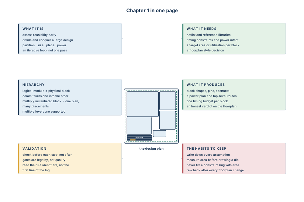
Where the next chapter goes, and why
You now know what a design plan contains, how to divide a netlist into blocks, how to size a core from measured area, and how to prove that a step is legal to run. Every one of those activities was described here as something you decide — and every one of them has to be typed into a tool that runs it, logs it, and lets you repeat it tomorrow without repeating the thinking.
That is the subject of Chapter 2. Before you can plan a real chip you need to be at home in the environment: the interfaces available to you, how commands are entered and interrupted, how to ask the tool about itself, how application options change its behaviour, how scripts and setup files make a session reproducible, where the command log lives when you need to reconstruct what you did, and how work is run in parallel and monitored when a design is too large for one process. Those are not administrative details. They are the difference between an engineer who can do this once and an engineer who can do it every day, on a design too big to hold in their head.