What are fin pitch, gate pitch, and contacted gate pitch in a FinFET technology?
From PDVerse PnR Interview Handbook · pdVerse Mentor Guide
Short Answer
Fin pitch measures the center-to-center spacing between neighboring fins. Gate pitch measures the repeat spacing between neighboring gates. Contacted gate pitch, often called CPP, describes a gate-repeat metric that includes the required contact arrangement.
Technical Explanation
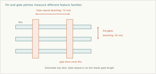
In a simplified top view, long parallel fins cross gate lines running in the perpendicular direction. Measuring between fins therefore measures a different direction and feature family from measuring between gates. A gate's drawn length along the current-flow direction is also different from the spacing between adjacent gates. These are distinct physical dimensions even when they all use nanometers. CPP and fin pitch help describe device density and constrain library layout, but they do not alone determine standard-cell area or routability. Contacts, diffusion breaks, power rails, local interconnect, pin access, and the cell architecture also consume space. A process-node marketing name is not a reliable substitute for any one of these measured pitches. For implementation, distinguish the device dimensions from the actual legal placement grid delivered by the technology and libraries. An ICC2 FinFET-grid report can have separate x and y pitch and offset values chosen for placement alignment. Do not assume its x pitch equals CPP or its y pitch equals fin pitch unless the technology methodology explicitly establishes that relationship.
Common Mistake
Using “fin pitch,” “gate length,” “CPP,” and “FinFET placement grid” as interchangeable terms.
Follow-up Question & Model Response
Why should a PNR engineer care about transistor-level pitches? They help explain library quantization and boundary restrictions, but placement legality must still use the delivered tool/library rules.
Practical Example
In an invented teaching layout, fins repeat every 40 nm and gates repeat every 70 nm. Those two measurements do not imply 40 nm wire width, 70 nm gate length, or a specific process-node name.
Continue practising