How do you inspect and debug the FinFET placement grid in ICC2?
From PDVerse PnR Interview Handbook · pdVerse Mentor Guide
Short Answer
Report the actual FinFET grid and run its dedicated check before changing geometry. ICC2's grid contains x/y spacing and offsets that guide placement of cells containing FinFET devices and can constrain relevant boundaries.
Technical Explanation
Use report_grids -type finfet to inspect whether the grid is defined and what pitches and offsets are active. Use check_finfet_grid to find reported violations. Read the affected object and boundary coordinate carefully: an error about a macro boundary is not necessarily an error about its origin alone. An origin can align while another boundary point fails because the dimensions are incompatible. For a simple coordinate check, subtract the applicable offset and divide by the pitch. The result should be an integer for a point required to lie on that grid. Perform exact DBU arithmetic where possible rather than relying on floating-point equality. Check both directions and any orientation-dependent boundary transformation, using the actual object rules rather than a generic formula alone. Fix the underlying cause: wrong technology data, incompatible macro abstract, mistaken unit scaling, wrong orientation, or an invalid placement. Moving one edge independently can distort a macro; rounding everything can damage other rules. Use approved grid-aware placement/floorplan operations and rerun the checks. If the grid is not defined, confirm the intended technology setup rather than inventing values.
Common Mistake
Copying grid values from a tutorial into a different PDK, or assuming a snapped origin guarantees all boundaries are legal.
Follow-up Question & Model Response
Why inspect both the database units and the grid? Conversion errors can create apparent geometry violations even when the intended physical dimension was valid.
Practical Example
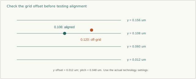
For an illustrative y offset of 0.012 um and pitch of 0.048 um, y = 0.108 um is aligned because (0.108 - 0.012)/0.048 = 2. A boundary at 0.120 um gives 2.25 and is off this grid.
Continue practising